My Apple II Rev 0 Replica Project
Fabrication
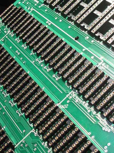
The PCB is made and the parts have been acquired. The next step is to put it all together.First step is to do a visual inspection looking for faulty traces. None were found.
Now I did a sanity check of the power and ground planes with no components installed. This involves basically checking for shorts between the various power supply sources and ground with a ohm-meter. I found no problems here.
Then I checked various components for fit. The only problem found here was a very tight fit for the expansion slot connectors. For my first board I slightly reamed out the holes in the PCB by hand with size 67 a pin vise. This was not enough to remove the plating in the holes, but allowed the pins to slide into the holes a little better. Note that this problem of tight fitting edge connectors has been solved in later kits by procuring edge connectors with smaller form factor pins.
On my first board, I now soldered in some components and connectors that had slightly odd configurations. This included the cassette interface, video, power and other connectors. Everything went well here. Since this worked out well, on future boards, I would leave these to last. The variable cap for color trim, the oscillator and the 200 ohm variable resistor were also soldered in during this phase, as well. On future boards, I will also leave these components to last.
Next up is the soldering in of the sockets. The key thing here is to check orientation and make sure that you don't put a 14 pin socket in a location for a 16 pin socket. My suggestion is to start with the biggest sockets, since you can't put a big socket into a location meant for a smaller one. Also make sure the sockets are fully seated when you first tack each corner down. I accomplish this by resting the socket in question on an small item with the weight of the upside down board holding it in. Otherwise you need three hands to hold the socket, the soldering iron and the solder itself.
Now recheck power and ground planes for shorts.
Now install the 44 decoupling capacitors and recheck power and ground for shorts.
Install remaining components and recheck power and ground for shorts, one last time.
Clean the back of PCB of excess flux. I discovered that Windex does a good job removing the rosin from the solder that I used. Your mileage may vary. Spray it on the back of the board and scrub with a soft brush that will not scratch the surface of the PCB. Next I cleaned up any remaining residue by running warm water over the back of the board while scrubbing lightly. Let dry overnight.
Check carefully for solder bridges while waiting for the PCB to dry.
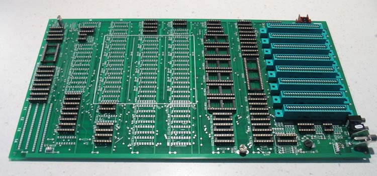
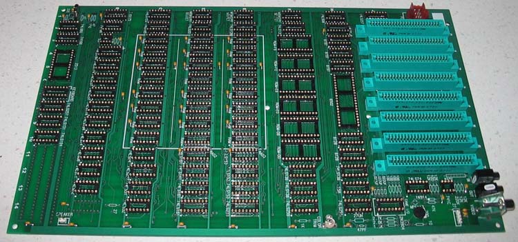
You can't really use an Apple switching power supply without a load, so at this point you need to stuff the majority of the board with ICs at this point.
Stuff the board with the ICs, but only stuff one bank of RAM and leave off Apple PROMs, for now.
Make up jumpers for memory configuration that you are interested in and insert those into memory select sockets.
You are now ready for bring up. Go to my bring up page for suggested sequence of bringup.
Back to Mike's Hobby Home Page