My Apple II Rev 0 Replica
Project
PCB Layout
This was the most interesting and
time
consuming
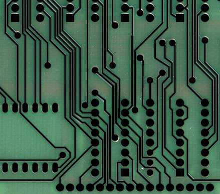
part of the replication process. The photo above shows shows a section
of a PDF
output of my layout overlaid over a photo of an actual REV 0 board.
I used photoshop to carefully align the replica layout
with
the original. This example gives an idea of how closely I've followed
the original layout. I've been lucky to obtain
quality
images of a rev
0
board from Geoff Harrison, which has greatly simplified the process of
recreating this design. In additional the famous "Red Book"
contains a
poor photocopy of the front a bare Rev 0 board, so that traces hidden
by mounted components can be followed and replicated.
See
the "construct your own replica" page for side by side examples of the
finished replica and an actual rev 0.
My
approach in producing the artwork was to use my Macintosh and an
excellent
program called Osmond PCB. There were several steps involved.
- Placement of components. Done by measuring existing Rev 1 board with calipers, as well as using semi transparent layers in Photoshop to compare postscript output of Osmond PCB with the Redbook photocopy of the Rev 0.
- Layout of traces. I could have gone another path here, but decided to not bother with creating a net list ahead of time. Instead, I've put down the traces as I went, with Osmond PCB. Osmond does export net lists, so before I went to fabrication, I exported and closely checked the final Osmond net list with schematics that exist in the "Red Book" and elsewhere. The layout of traces was very time intensive, since I attempted to reproduce the exact rev 0 board layout. It was especially hard to determine the path of some traces that went under components and were in areas not well reproduced by the PCB scan in the Red Book. However, with patience and by examining a Rev 4 board, which has largely the same layout, I believe I've been able to replicate even these paths with good accuracy. In one case, I even cut out part of a socket on that rev 4 board in order to determine how a trace was run on that board. Once again the layers feature in Photoshop is used to verify correct placement of traces.
Here is some interesting data that I have gathered in the process of laying out the board.
Mistakes found
Other than the 20/24K addressing bug and the issue with cassette output signal. Apple's rev 0 copper layout was remarkably bug free. However, I found a couple of small things during my layout process that might be considered small errors.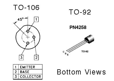
- Transistor layout in clock generation logic is setup for a 2N4258 in a TO-106 package. The TO-106 package is an older package type. These days this package type is usually only seen in photo-transistors and back in 1977, it was rapidly falling out of favor. Every original board I have seen has the 2N4258's in a TO-92 package. It turns out that either package can be made to work with this layout, though the orientation of the silkscreen and placement of the holes is incorrect for the TO-92 package.
- These same transistors are not labeled on the silk screen. These are the only devices on the board, except for decoupling caps that are not labeled.
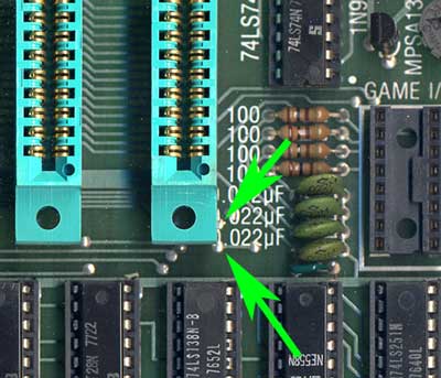
- Only three of the four .022 uF caps near the game port are labeled.
- Later revisions straightened a number of traces that were unnecesarily crooked, but I wouldn't consider these real mistakes.
Unexpected differences between Rev 0 and Rev 1 motherboards
- NC (no connect) on pins 35 and 19 of 50 pin Apple II bus appears to be actually connected between the I/O slots. I believe that this was changed in rev 1 boards, in order to allow slot 7 to accept video signals for the PAL color board (see expected differences). This is interesting, because even the "Red Book" documents these as not connected.
- After reset, a spurious character is entered into the keyboard input buffer. This issue is documented in the Apple II Reference Manual, but I didn't realize the problem existed until I started seeing it when operating my rev 0 replica. The manual says to type cntrl-x and return to delete this unwanted character. This problem occurs even if you have a disk II controller in your system with it's reset circuit. The reason is that reset is not connected to clear the keyboard strobe. The keyboard strobe is connected to the flip-flop's clock input. The flip-flop is configured to set it's output on the clock's rising edge. The strobe input must normally go high sometime during power on causing the flip-flop to be set during every power on.
- Not well documented are the improvements to the horizonal and video sync signals made in the rev 1 motherboard. Some monitors (including some Apple composite monitors) will have trouble with horizontal sync lock (distortion seen at top of screen) with rev 0 boards. I have a page with more information and a couple of fixes for this issue.
Expected differences between Rev 0 and Rev 1 motherboards
- NC 35, slot 7 is connected to video circuitry in REV 1
- For Rev 0, H1-3 is connected directly to E2-15 (addressing bug for 20k & 24k systems)
- No power on reset circuitry in Rev 0 - a disk II controller contains a power on reset circuit, so you will not notice this if you have a Disk II installed in your system.
- Slight difference in cassette input op amp configuration.
- Hires graphics mode only support 4 colors
- No color killer circuit for text mode
- Rev 0 has no provisions for conversion to 50HZ PAL operation
Errors in Schematics in Red Book!
I found that these schematics are incomplete with the soft-5 (A2-8 and A2-11) inputs to various chips are not documented. In other places connections to GND are not documented.- S-2: 6502-38 goes to GND, not 6502-28 to GND on processor
- S-6: C12-9 is connected to J1-2, not J1-5 & H1-11 is connected to J1-5, not J1-2
- S-6: E2-3 is connected to J1-4, not J1-7 & E2-2 is connected to J1-7, not J1-4
- S-6: J1-1 is connected to Clk 0, not Clk 1
- S-8: E12-9 is connected to A4, not E12-7
- S-8: E13-9 is connected to A5, not E13-7
- S-9: H2-5 is clock 1 not clock 0
- S-10: F13-14 is connected to B10-13, not B10-10
- S-10: F13-13 is connected to K13-11, not K13-1
- S-10: +5 is connected to 741-7 and -5 is connected to 741-4
- S-11: A8-12 is connected to A10-4, not A10-3
- S-11: A8-7 is connected to A10-3, not A10-4
- S-11: 2513 is connected to -5 (pin 12) and -12 (pin 1)
- S-11: R9 is connected to +5V, not -5V
That Mysterious USER 1 Jumper
The top via connects to USER1 which is connected to pin 39 on all the edge connectors. The bottom via connects to H12 pin 6, which an enable input to the I/O address decoder. This enable input is normally pulled up to +5 volts by one of the 3K resistors in the SIP near slot 7. Connecting these two vias connects the USER1 signal from the bus to an enable input of the decoder at H12. If driven low, I/O decoding is disabled, except for the on board ROMs. I suppose this could be used to reuse some of the I/O space used by onboard I/O devices. As far as I know this capability was never used by any production I/O card. USER1 was reused on the Apple IIe as 65C02 SYNC and once again for M2SEL on the Apple IIgs.
Confusion About Rev 0 Statements in Jim Sather's book "Understanding the Apple II"
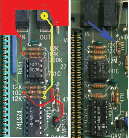
- In this book, it is stated that one of the improvements made to PCBs after the rev 0, was that the speaker output was disconnected from the cassette output. After being confused about this statement for a while, I've come to the conclusion that this is a board layout issue, not a logic problem. I believe that noise was picked up from the speaker signal ground trace that runs by the 100 ohm resistor on the rev 0 boards. In the photo above, red and green highlights the ground path from the speaker amplifier. Yellow highlights the cassette output, which is connected to the speaker amplifier ground by a 100 ohm resistor. The blue arrow on the right highlights how the 100 ohm resistor from cassette output to ground was relocated to avoid picking up noise from the speaker ground.
- He also states that the cassette input amplifier was redesigned. After looking at the changes, I think the changes were fairly small, hardly something that would normally be considered a redesign.
Overall Impressions
First of all, digitally recreating a board of this size that that was laid out by hand is no simple process. I estimate that I spent an average of 10 hours a week for 4 months on this. I might have spent much more time than this, but I don't really want to know if that is the case. Grant Stockly on his Altair Kit page recommends using a PCB scanning service for such tasks. I didn't have a rev0 to start with, and if I did, I would have been reluctant to rip it apart to get a good scan.However lengthy the task, it could have been far harder than it actually turned out to be. It was quite remarkable how the vast majority of the 15 mil traces lie precisly on a 25 mil grid. The majority of the traces that run diagonally, run precisely at a 45 degree angle. The chips are in precisely alignment and best of all, there were only two layers to contend with. The square ends on some of the power and ground feeds were tricky to contend with in Osmond, but eventually I figured out a way to get it right.
I ran across a few odd things during the process. A few of the pads on the bottom side of the board were smaller than normal to allow traces to slip between them. Check out slots 0 & 6 and ICs D2 and A8 for examples of this. One of the hardest portions of the recreation, was the silkscreen. I can understand why Grant Stockly didn't recreate the original silkscreen on his Altair Kit, though he had a very poor silkscreen to start with, compared to the Apple II.
Back to Mike's Hobby Home Page