First a look at the back of the chassis with the 78S11 sockets mounted. I don’t have the 86CP4 power socket installed. That will come later.
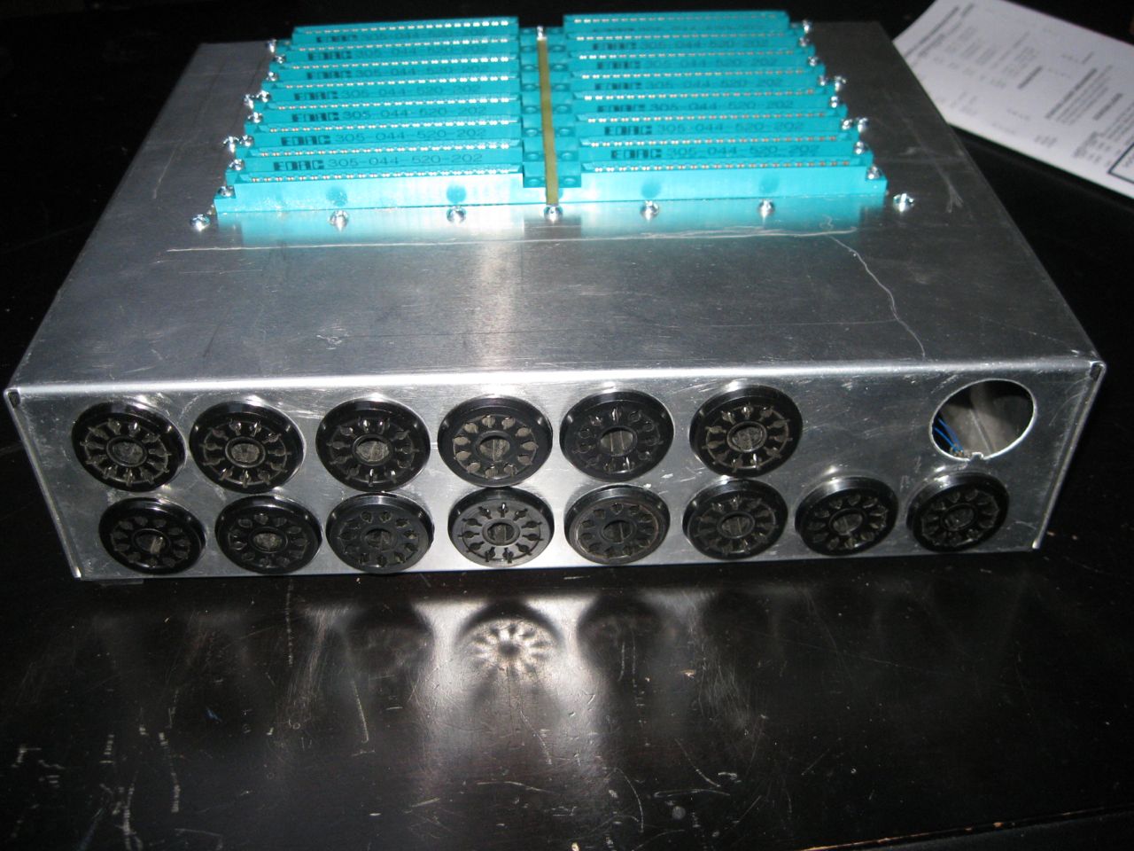
Chassis with 78S11 Sockets
Now a view of the completed I/O wiring.

Chassis I/O Wiring
This is a lot of work. A ground wire is connected to pin 11 of each port. This is 14 wires.
The output ports have 8 bits bussed directly from the data bus that goes to the SRAM slots to all the sockets. Plus another strobe line is connected for each port from the DBB card. I imagine any output device would be designed to latch output data when it sees the strobe for the connected port. This is 8×8 + 8 or 72 wires
The input ports have 8 bits of data connected separately for each port directly to the input card. This is 8×6 or 48 wires.
Total number of wires 14+72+48 = 134 wires. I have noticed that at least one original SCELBI had only the first two input ports wired. I’m guessing the builder thought that two would be enough for now, and if he needed more, he could add them later.