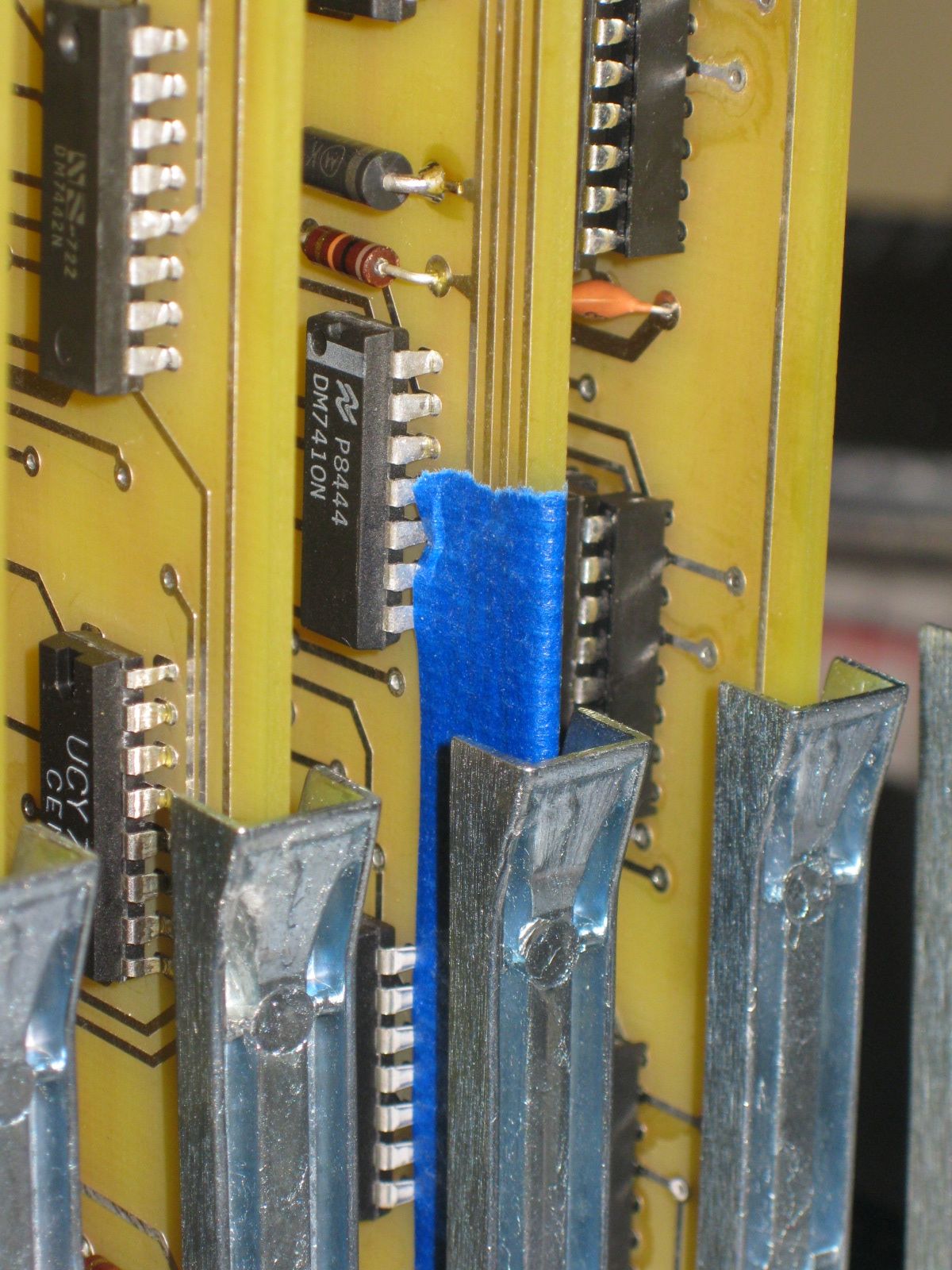
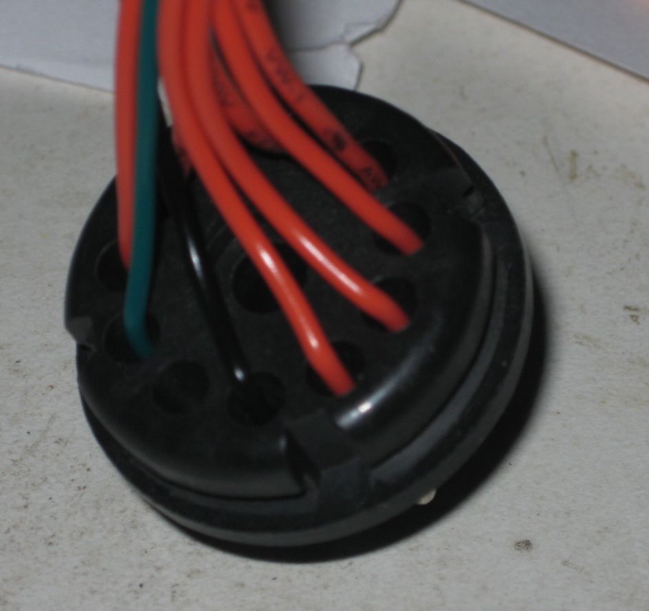
The SCELBI has 8 output ports. Each port is implemented with an Amphehol 11 pin 78S11 female socket. The sockets are still available, but tend to be expensive, often $12 or $13 dollars or more. Each port is connected to the SCELBI 8 bit data bus (pins 1-8), system ground (pin 11) and a strobe signal (pin 9). Pin 10 is left unconnected.
The 8 bit data bus, as the name suggests is bussed across all 8 output ports and to the rest of the computer. The ground is also connected to the backplane system ground. The strobes are unique for each port. This is, in fact the only difference between each output port. Output hardware must latch the data bus when the strobe signal is seen on that port.
The mating plug is another expensive connector, called an 86CP11. Here are front and back images of an 86CP11.
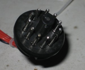
front 86CP11 plug

Back 86CP11 Plug
It took me a while to figure out how to solder wires to this connector. I used 22 gauge solid conductor hook up wire. You strip about 3/8″ from one end (give or take) and stick the wire into the tip from the back of the connector until the conductor comes out the little hole at the end of the tip. I then bent the conductor over a bit so it wouldn’t slip back in and soldered from the tip of the plug. Then I carefully cut the excess conductor off. I’m sure some old hand will send me an email, saying how I’m doing it all wrong, but it worked for me.
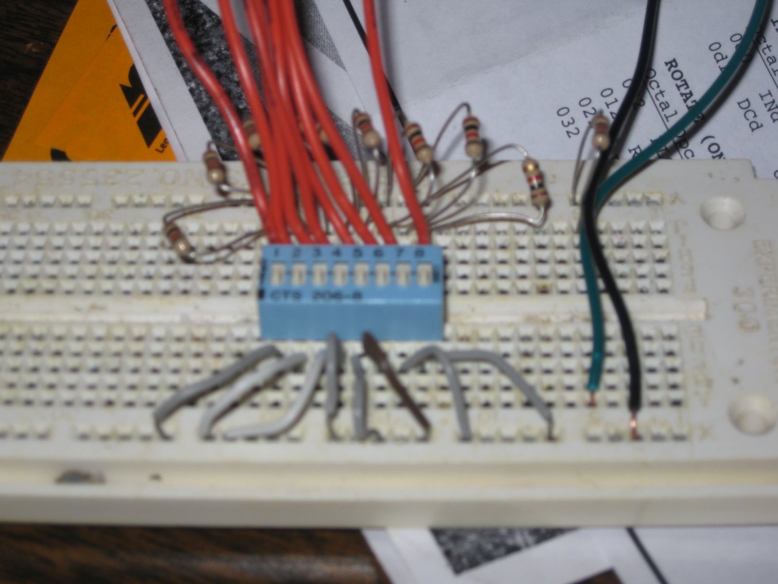
I didn’t have 10 different colors of wire, so I used black for ground, red for the 8 data lines and green for the strobe.
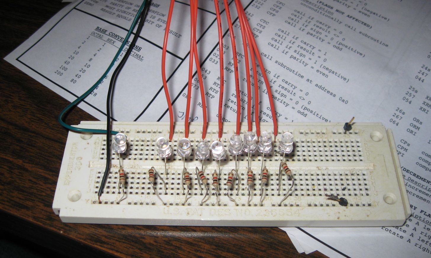
For output port testing purposes, I connected the other end of the wires to breadboard. Each wire was connected to a LED which was connected to ground through a 1K resistor.
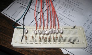
Output Port Test Rig
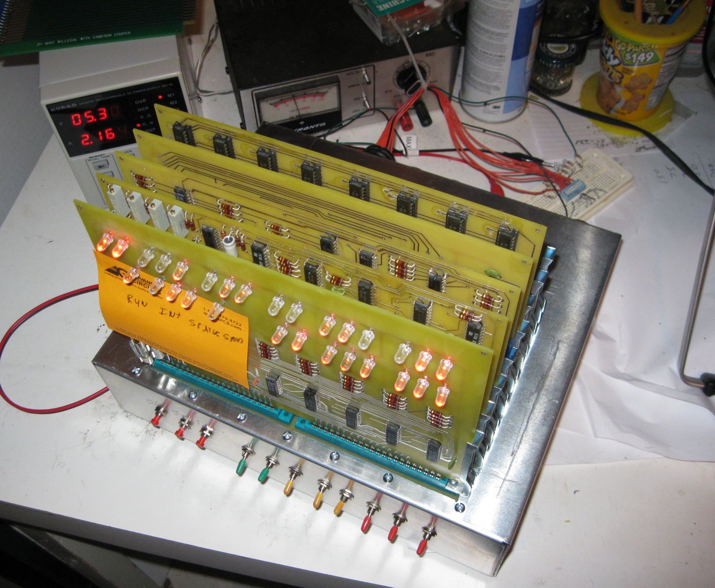
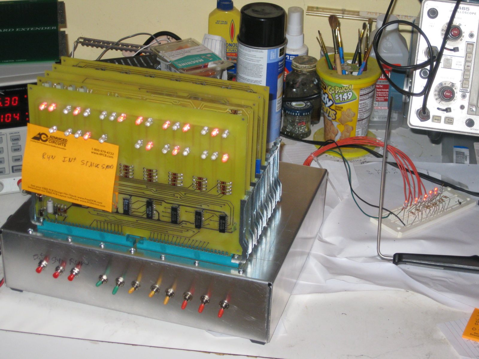
Now by writing data to the output port, I visually check each line, including the strobe, by executing simple code fragments. I plugged the test rig into port 0 and powered up the SCELBI. I loaded this simple code fragment into memory, starting at location 0.
OUT 0

JMP 0
Next I manually loaded the accumulator with the data I wanted to write by jamming in a LAI instruction and then jammed a JMP 0 instruction. I then stepped through the little loop, watching the LEDs on the test fixture. I then tried a few other data patterns by putting different patterns in the Accumulator and rerunning the test. Then I moved the connector to the next output port and loaded location zero with the OUT 1 instruction. I repeated the test for this port and the remaining output ports.

Output Port Test
Everything checked out perfectly and I’m declaring the output port logic in perfect working order.