
While fabricating another SCELBI-RS232 PCB I did some experiments with transferring the toner to the PCB. After some less than stellar transfer attempts, I got a good transfer and etched this board.
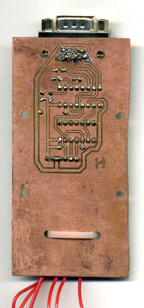
SCELBI-RS232
You can ignore the mess around the DB-9 connector, that was the result of soldering with too big of soldering iron tip in that tight space. As you can see the circuit is very crisply etched. The circuit has a lot features with 10 mill spacing, for example, the smilely face has 10 mill lines with 10 mill spacing to the flood area.
I accomplished a good transfer by reducing the heat setting on my iron and making the transfer in less than a minute. I used to use maximum heat and really use a lot of time and pressure to iron on the toner. This often resulted in embedding fibers of the paper in the transfer, so I decided to experiment with backing off on heat. I decided it was better to just use enough to melt the toner to make the transfer. I use paper from glossy magazines, my favorite being National Geographic, which seems to use a little heavier paper than some other publications. The low cost of redoing a toner transfer means you should experiment with these techniques until you get a solution that works for you.
Once I got a good transfer for the copper layer, making a silk screen transfer was pretty easy. Apply the silk screen after etching the copper, but before drilling.
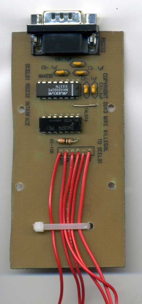
SCELBI-RS232 Silk Screen
Exactly the same thing I discovered when reproducing the Cyclops PCB from Popular Electronics. Nat Geo pages (especially old ones) work best because they use (used?) a clay based printing process.
Bill