
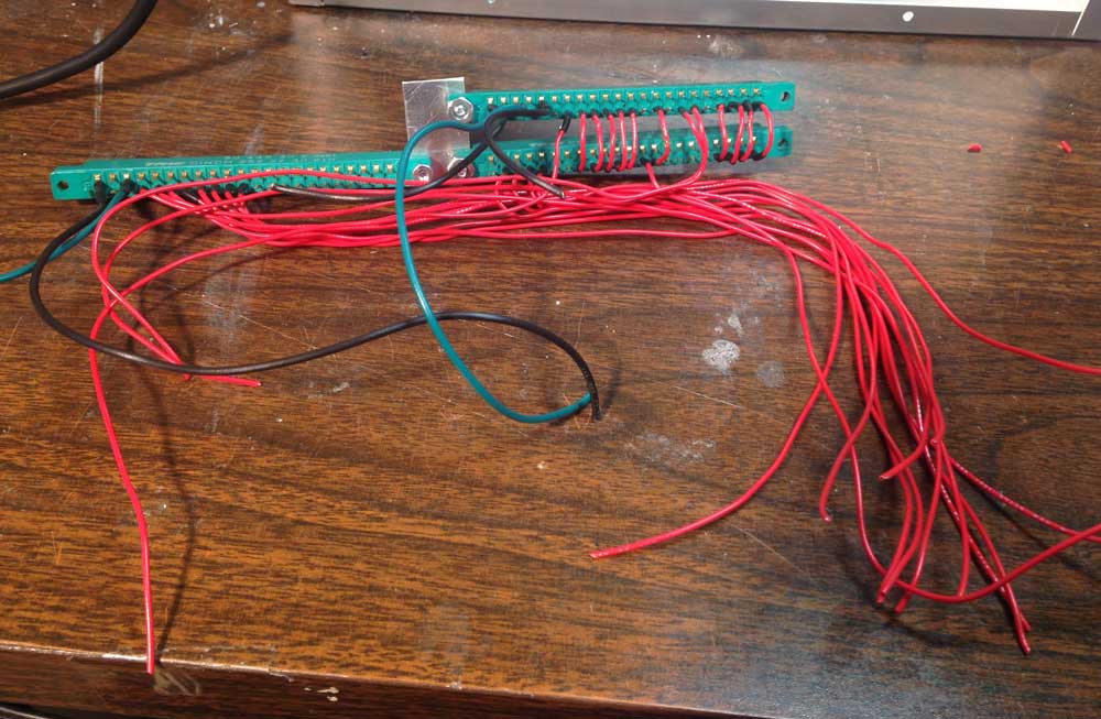
Edge Connectors Wired
I have the edge connectors wired and ready to go into the chassis. It should be apparent why I wire these connectors before mounting them in the chassis.
The original unit used wire wrap, but I had these connectors on hand, and decided to solder the wires on, just like the cassette and tty interfaces.
If you follow the schematics, most of the connections are pretty apparent. However sync (BP) and the four strobe inputs (BB, BC, BD, BE) are not. Turns out that sync will go to pin 10 on P1. Out 0 on the main chassis needs to be connected to sync, just like needed to be done with the cassette interface. From studying the images I have, I think that the strobe inputs are spread out between pins 9 and 11 of both P1 and P2. Pin 11 is ground and pin 9 is the strobe output of each port. In this case, the ground inputs of the P1 and P2 connectors are not used as a system ground connection, but only as a low logic input connection. There is some chance that I will have the P1 and P2 outputs swapped compared to the original unit, but without original software or access to the original hardware, I can’t tell for sure which port was connected to which input latch.
I think when they built the chassis for the oscilloscope interface, they should have swapped the ports and the oscilloscope connectors. This would have reduced the length of a number of wire runs. Who knows, maybe they did make that change on later units, but unfortunately no others are known to exist.