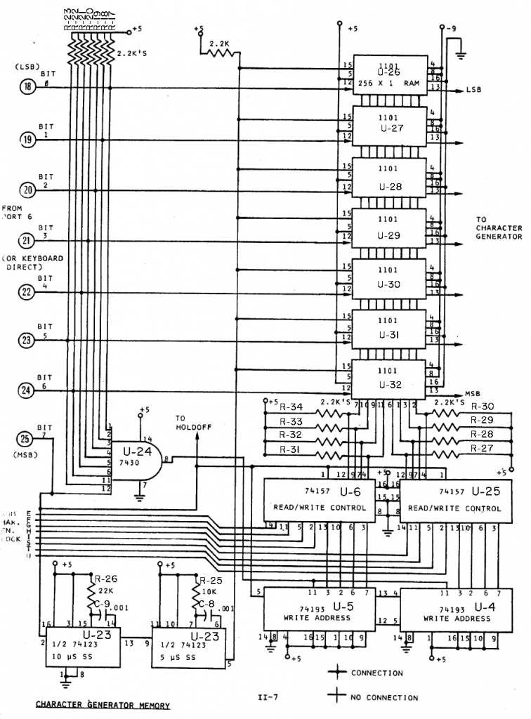
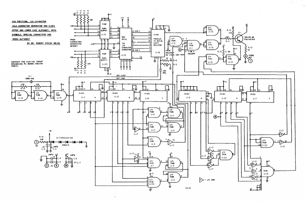
These schematics have part identifiers added to them that match the drawing that I posted yesterday. There are also a couple of corrections. A couple of the connections to the inverters at U-17 and U-21 went to different pins than what was actually connected on the PCB. No functional difference, but it could cause some confusion when debugging. One other thing, there are actually eight voltage dropping diodes, not the five shown on the schematics.