
This PCB layout is now in it’s fifth major revision and counting. Here is how it’s evolved.

A2 Hobbyboard Layout
1) A direct copy of Apple’s Hobbyboard. Many years ago, I used one of these cards to build an A/D interface with temperature sensor. This layout is ideal for prototyping with wire-wrap technology, but not so good for point to point wiring, which I prefer these days. So I moved on.

A2 Shutter Tester on QRC proto board
2) A direct copy of a Quality Resarch Company (QRC) Apple 2 computer prototype board. I used one of these a few years ago to build a prototype shutter tester. This board is ideal for point to point wiring, but I have decided it would be neat to build into the layout some basic I/O components like space for a 2K PROM and data bus transceivers.

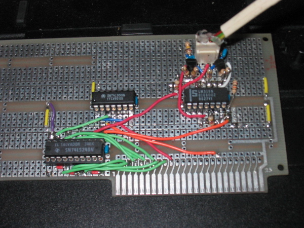
The first proto design of my own making
3) This led to the first of my own designs. I incorporated space for a bus transceiver, a 27C256 EPROM, a SPDT switch and a DB 9 connector in this one. I used the 27C256 instead of a 27C16 because they are easier to find and cheaper, despite the fact that it has 16 times as much memory than is really needed. However, the handing of the I/O strobe for the 2K memory exansion space is kind of messy. On Apple’s super serial card, it takes 4 74LSXX series chips. This would require a lot of wiring and take up a big piece of the proto area. For these reasons, I decided to put this logic in a PAL or GAL and include the wiring right on the proto board, which leads to my next design.

My Second Proto Design
4) In this version, I removed the toggle switch, thinking that it was not really that useful an idea. I was thinking I wanted the capability of interfacing an AVR micro-controller, while some other folks thought that a design that supported classic chip would be more appropriate. The 6522 VIA is a classic 6502 family part and includes some neat features including built in timers. I also switched from using a 27C256 to 28C256 flash part, so that it could be programmed in place, without the need for a PROM programmer. All along, I’ve wanted the capability of supporting that AVR on this board, but supporting both a micro-controller and a VIA seemed kind of awkward on the same layout.

Third Proto Design
5) My current layout tweaks the previous by making the half of the 6522 that is used for input/output pins a little more generic. The 6522 will still drop right in, but if something different is desired, then you just need to connect the bus interface to the proto area the way you want it. It is fortunate that the 6522 was set up with the I/O ports on one side of the chip and the bus interface on the other. In some ways, the 6522 VIA bus interface is just about an ideal generic A2 interface device. You have the system clock, the device select signal, read/write, interrupt, the data bus, and the four address lines that will address all 16 locations in the device select region of each slot. If you need some other bus signal, it can always be picked up off of the pads near the edge connector. One of my next challenges is to see if I can interface an AVR micro-controller directly to this bus, without additional components.
This design is not done evolving, but at this point, I think I’m happy with most of the major design decisions. I have plenty of FLASH memory for the program, a 6522 VIA for hardware interfacing and DB-9 for connection to the external world. With the 6522 in place, I have space for 4 16 pin chips, an 8 pin chip and plenty of discrete components. Yet the 6522 could easily be replaced by something else, like the AVR I keep thinking about.
One thing that might change is the DB-9, which takes up a lot of real estate. A KK type header like the one used on the super serial card is likely to replace it.
If you have ideas or opinions on this hobbycard design be sure to let me know. The more input I get, the better this card is likely to become.