
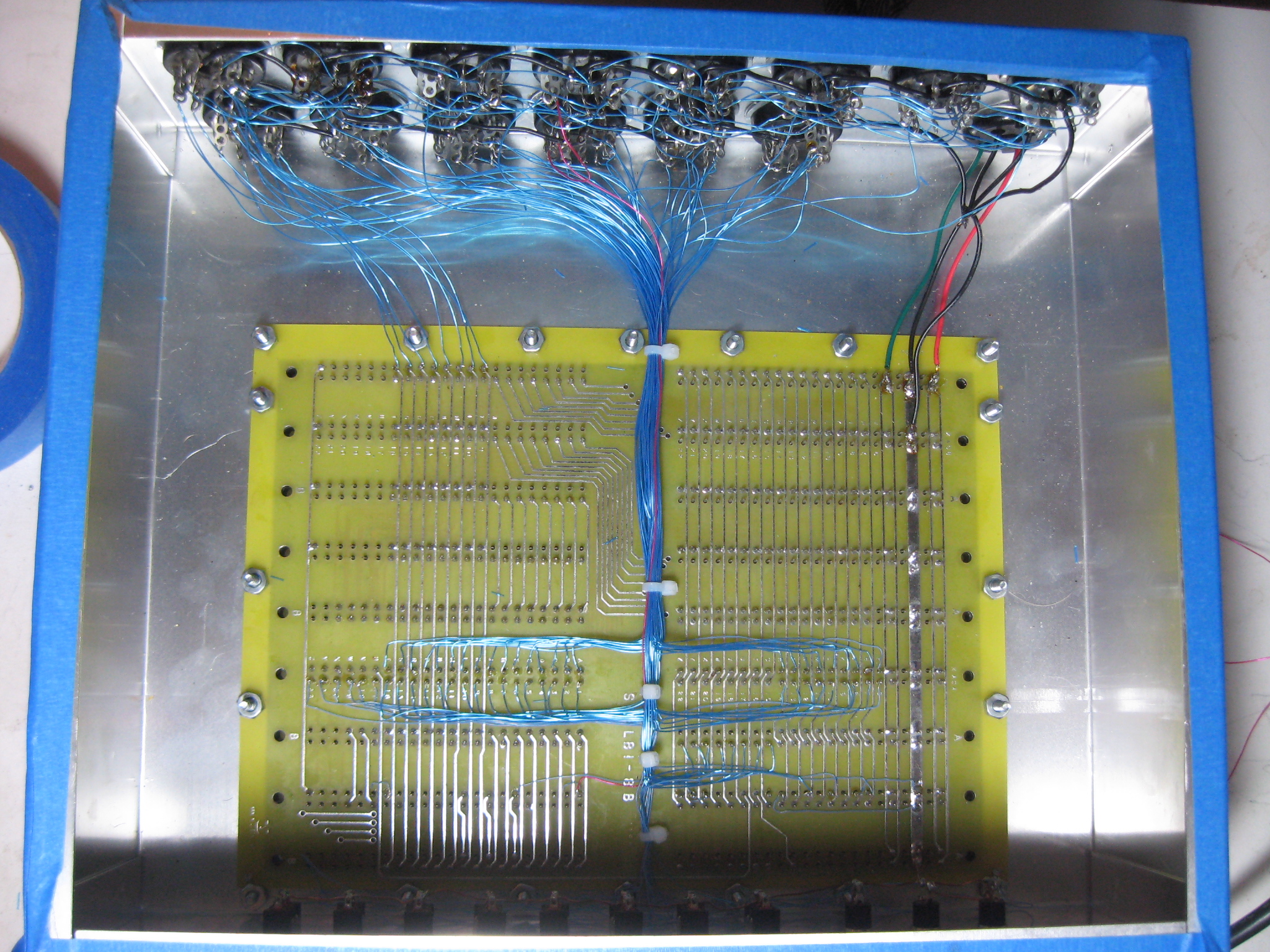
SCELBI 8B Wiring Complete
I decided to wire the data output bus to the end connector rather than split between the middle two connectors as specified in the SCELBI build manual. I choose to do this primarily because of the cleaner wiring that is possible. The way the data bus is connected to all the memory cards, all the I/O ports and then to connected peripherals through long cables, leaves lots of room for transmission line issues. This concern, is probably why SCELBI recommended connecting four bits to each of the two center connectors. I’m no expert on transmission line theory, so I’m not sure whether the end connection will cause any issues that will require redoing this particular wiring. My guess is that given all the other wiring and relatively low data rate, is that it will have no measurable affect, which is why I’m trying it. The other thing about it, is the idea that I picked up somewhere along the way that branching transmission lines is generally a bad idea. I suppose I’ll have to compare my 8H which was done the SCELBI way with the 8B and see which looks cleaner, electrically.
The other thing I’ve done, is to connect the CPU SYNC clock to pin 10 of input port 3 and pin 10 of output port 3. These are the two red wires, one down the middle of the backplane, and the other from input port 3 to output port 3. Based on my examination of the SCELBI cassette schematics and drivers, it looks like this will be needed to provide timing for the cassette interface.
The last two items before moving onto the cassette interface is checking out the system, now that the I/O is wired and then, finally, screen printing the front panel. I did try screen printing a panel a week or so ago, but had issues with my screen not being stretched tight enough and I’ll have to make another one.