SCELBI Oscilloscope Edge Connectors

Edge Connectors Wired

Edge Connectors Wired

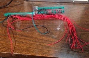
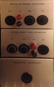
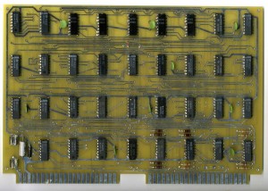
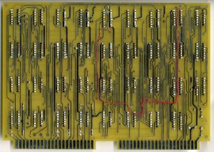
I have the edge connectors wired and ready to go into the chassis. It should be apparent why I wire these connectors before mounting them in the chassis.

The original unit used wire wrap, but I had these connectors on hand, and decided to solder the wires on, just like the cassette and tty interfaces.

If you follow the schematics, most of the connections are pretty apparent. However sync (BP) and the four strobe inputs (BB, BC, BD, BE) are not. Turns out that sync will go to pin 10 on P1. Out 0 on the main chassis needs to be connected to sync, just like needed to be done with the cassette interface. From studying the images I have, I think that the strobe inputs are spread out between pins 9 and 11 of both P1 and P2. Pin 11 is ground and pin 9 is the strobe output of each port. In this case, the ground inputs of the P1 and P2 connectors are not used as a system ground connection, but only as a low logic input connection. There is some chance that I will have the P1 and P2 outputs swapped compared to the original unit, but without original software or access to the original hardware, I can’t tell for sure which port was connected to which input latch.

I think when they built the chassis for the oscilloscope interface, they should have swapped the ports and the oscilloscope connectors. This would have reduced the length of a number of wire runs. Who knows, maybe they did make that change on later units, but unfortunately no others are known to exist.

SCELBI Analog Board Power Supply Installed

Power Supply Installed

Power Supply Installed

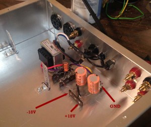
This took a bit more time than expected, but at least the result is a little cleaner than I really hoped for.

I’ll wire the digital to analog board connections next. After that I’ll attach the power supply and external interface wiring to the edge connectors. I’ll mount the edge connectors in the chassis and connect the dangling power and interface wires to the appropriate connectors. I expect this to be pretty straight forward and go faster than all the previous steps to this project.

I’m not sure if I mentioned it before in this blog, but building the SCELBI Oscilloscope Interface is more complicated than building some basic computer systems.

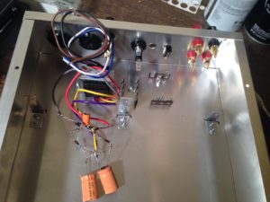
Scope Chassis ready for wiring

Inside Repro Oscope Chassis

Inside Repro Oscope Chassis

I bought several versions of terminal strips only to use a 4 postion version from Antique Electric Supply. I ended up cutting them down to make the three position set.

I’m going to wire up the power supply first, then wire in the edge connectors. Note that one side of the transformer shares a mounting screw with a terminal strip. Also, on the original unit, the edge connectors are mounted on a panel and secured to the mounting brackets. At the moment, I don’t have enough stock to make a full panel, so I’ve made a mini panel, and I’ll retrofit a full panel later on.

SCELBI O-scope Opamp Power Supply

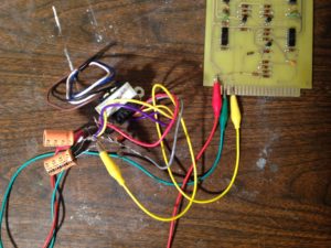
Here is a view of my version of the SCELBI O-scope Opamp Power Supply test setup. AC power is not connected in this photo, but would be connected to the transformer during the actual test.

Opamp Power Supply

Opamp Power Supply

I’m using a Triad VPL28-180 transformer and 1N4002 diodes. I found the diodes in my spare parts stash. The first smoothing capacitor is rated at 100uf/50 Volts. The +18 and -18 supplies have 470uF/25 volt smoothing capacitors. The latter are probably overkill, but it’s what I could find in my spare parts stash. The resistors are rated at 120 ohm, 1/4 watts. The zener diodes are the BZX79C18 that I mentioned in a previous post.

After hooking up to the analog board, the voltages are within a volt of +/- 18, with no measurable ripple. Transformer output is a little higher than with the original transformer that I tested with, but not enough to be of concern. Zener shunt current is OK, so I’ll just move this set up into the enclosure, without changing any components.

SCELBI O-scope Chassis Progress

Well there is a reason why I changed majors from mechanical engineering to computer science.

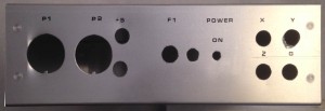
SCELBI Oscope Front Panel

SCELBI Oscope Front Panel

A few imperfections in execution, but it will look fine when the connectors and switches and such are added. This is a Bud AC413 chassis, the original chassis was constructed a bit differently, and 1/2 inch higher. I didn’t notice the Z and G when making out the rub-on artwork, but fortunately I included some extra text including an extra “GND”. The N turned sideways makes a decent Z.

I have a few more coats of clear lacquer to spray before moving onto the next stage.

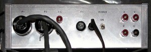
For Comparison, the following is an image of an original SCELBI O-scope Chassis taken by Jack Rubin. It has been slightly photo-shopped to fix the perspective.

SCELBI Oscope Original Front Panel

SCELBI Oscope Original Front Panel

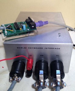
SCELBI Keyboard Interface All Hooked Up and Running

SCELBI Keyboard Interface All Hooked Up and Running

SCELBI Keyboard Interface All Hooked Up and Running

For now, I’m using one of my PS/2 adapters (on top of the enclosure) to connect to a PS/2 keyboard. I was going to cobble together a cable for my reproduction Datanetics keyboard, but it requires -12 volts, which would have to be generated separately just for this keyboard.

Now I can focus on the Oscilloscope Interface.

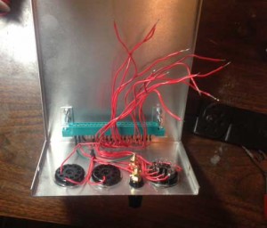
Wiring the Keyboard Interface Enclosure

Wiring the Keyboard Enclosure

Wiring the Keyboard Enclosure

At this point, I decided to call it a day and said to myself, my next project isn’t going to involve so much point to point wiring. Counting both chassis, the peripherals and cabling, I must have soldered about 500 point to point wires during the course of the SCELBI project.

By the way, I think the best process for constructing one of these enclosures is as follows.

  • cut and drill the holes
  • add the rub on lettering
  • clear coat the lettering with lacquer
  • add the connectors
  • wire it
  • There are 12 wires left to connect on this chassis.

    For the oscilloscope interface checkout, I think I’m just going to build it up in the chassis, rather than test it and then make the chassis.

    SCELBI – Oscope Digital Board

    OSCOPE DIGITAL PCB - front - with rework

    OSCOPE DIGITAL PCB – front – with rework

    SCELBI OSCOPE DIGITAL PCB - back - with rework

    OSCOPE DIGITAL PCB – back – with rework

    Notice that I have also recreated the rework. Note that the proper way to cut a trace on a PCB, is to use a sharp hobby knife to make two parallel cuts in the trace an 1/16″ or so apart. Then you remove the small piece of copper between the cuts.

    The Analog board has also been built. What’s left is wiring up the board edge connectors to power and amphenol connectors.

    Scope Analog Power Supply Part II

    Before I finalize on values for the SCELBI scope analog supply components, I needed to know how much power the board consumes. To determine this, I set up two bench supplies to power the board and measure current consumption.
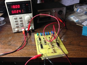
    Scope Analog Board Current Test

    Scope Analog Board Current Test

    Current consumption on both positive and negative rails measures at only about 25 mA. It’s possible current could vary a bit when hooked up to scope output and the digital board for input, but looking at the schematic makes me think that it’s not going to change very much.

    The way this zener based regulator works, is that if the voltage is over 18 volts, the zener shunts current to ground causing a voltage drop over the series resistor. The zener selected has to have enough current sinking capability to shunt the excess current to control the voltage. The resistor has to have enough current capacity to sustain the current for the entire circuit.

    With the 28 volt transformer I found in my stash, the rectified DC voltage with no load is about 22 volts. The formula for finding the amount of current that the series resistor must handle is simply ohms law. Here is the formula for the 150 ohm resistor found on the original power supply.

    I=V/R
    V= 22-18
    R=150
    I= (22-18)/150
    I = 4/150
    I = .026 AMP
    I = 26 mA

    Here’s the tricky part. For a zener to regulate correctly, it must pass a minimum amount of current. The current, the series resistor passes, will be split between the zener and the board. If the board consumes 25 mA, then almost the entire drop of 26 mA over the series resistor is due to the board, not the zener and the zener will only be passing 1 mA. I checked the data sheet of a typical zener, the Fairchild BZX79C18 and it is specified at 5 mA. 1 mA may not be enough to regulate the voltage well, at least for that part. Either a larger input voltage coming from the transformer or smaller series resister will be required, if I was to use a BZX79C18.

    If I switch to a 120 ohm series resistor. The formula looks a little more promising.

    I = (22-18)/120 = .033 AMP
    I = 33 mA

    With the board consuming 25 mA, this leaves 8 mA for the zener to shunt, which should be enough, at least for the BZX79C18.

    I don’t have the specification for the original power supply’s transformer, which may account for the slightly different series resistor value of 150 ohms that is in the original device.

    The wattage capacity of the series resistor and the zener is also important. The formula for watts is simple W = I x V. First for the resistor.

    W = I x V
    W = .033 x 4
    W = .132 watts
    W = 132 mW

    Assuming my other calculations and measurements are correct, even small .25 watt resistors should be sufficient for this application.

    Then for the zener

    I = .033 – .025 (the board consumes .025 Amps, which is not shunted through the zener)
    I = .008
    W = .008 x 18
    W = .144 watts
    W = 144 mW

    The BZX79C18 is rated at 500 mW, so it also should be fine for this application.

    With the low current requirement for this power supply, I’m going to pick up a smaller transformer, as the 1 AMP transformer I had in my parts stash, is clearly overkill and will not fit in the oscilloscope interface enclosure.