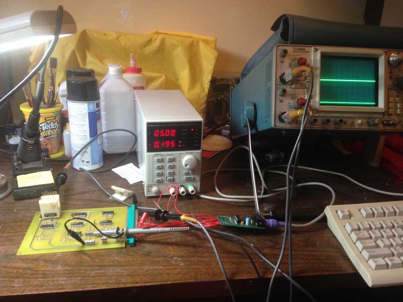
SCELBI Keyboard Interface Checkout
This setup is being used to checkout basic functionality of the SCELBI Keyboard Interface card. The card was designed to interface to a Don Lancaster Keyboard as described in a couple of articles published in Radio-Electronics in 1973. The first article was the February issue and contained instructions on building a basic non-encoded keyboard. The April issue contained a follow on article with a description on how to build a keyboard encoder. These links contain the original articles and are hosted on Michael Holley’s comprehensive SWTPC pages. This keyboard/encoder design does not latch keypresses, but simply outputs what it sees, as the keystrokes occur. The strobe is supposed to come after the keyboard data, and end prior to keyboard data, so interfacing hardware doesn’t have to do anything fancy to latch the data.
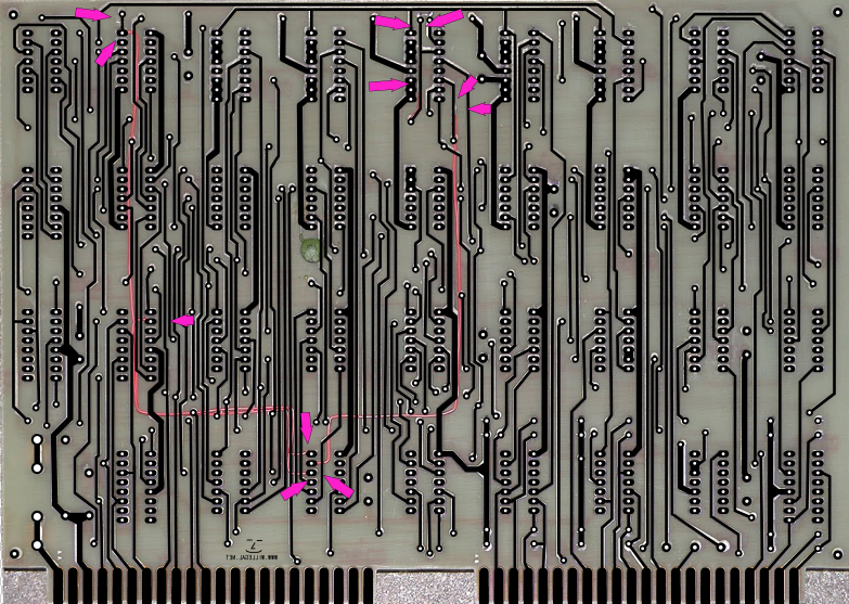
The SCELBI keyboard interface accepts 8 bits of input data from the keyboard, with the most significant bit (MSB) being a strobe. The interface to the SCELBI computer contains 8 bits of data, with the MSB being a data available indicator. The data available indicator is cleared by a single input (high to clear) from the computer. The data and strobe coming from the keyboard can be independently inverted or not, by correct selection of jumpers around Z1 and Z4 and inclusion of the Z1 and Z4 7404 inverters or not. Leaving the 7404s out and bypassing them with jumpers will result in inverted data. With my PS/2 keyboard adapter, I needed to use the 7404 to keep the interface from inverting data. At one time, I had a version of PS/2 adapter firmware that would invert data, which would have been handy in this case, but I removed that feature some time ago.
It appears that SCELBI engineers had trouble using the Radio-Electronics keyboard strobe to latch data correctly. The strobe is OR’d with the data bits in order to make up an internal strobe for use within the board. Many keyboard designs internally latched data, and this extra circuitry doesn’t work since the incoming data never goes away, and the strobe stays stuck on. For my testing, I used one of my PS/2 adapters. I considered two solutions to this problem with strobe. My first thought was to modify my PS/2 keyboard adapter firmware to make it emulate a non-latching keyboard. In the end, after playing around with the interface, I decided to simply delete the gates that OR’d keyboard data with strobe. This can be seen in the following photo as the deletion of IC Z7 and the jumper from the pad at pin 2 to the pad at pin 12.
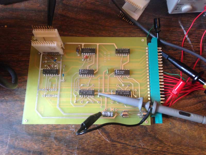
Configured Keyboard Interface
With this simple modification, I have bench tested the keyboard interface to the extent possible. Next, I need to write a small 8008 keyboard driver and connect to my reproduction SCELBI 8H.