SCELBI boot loader

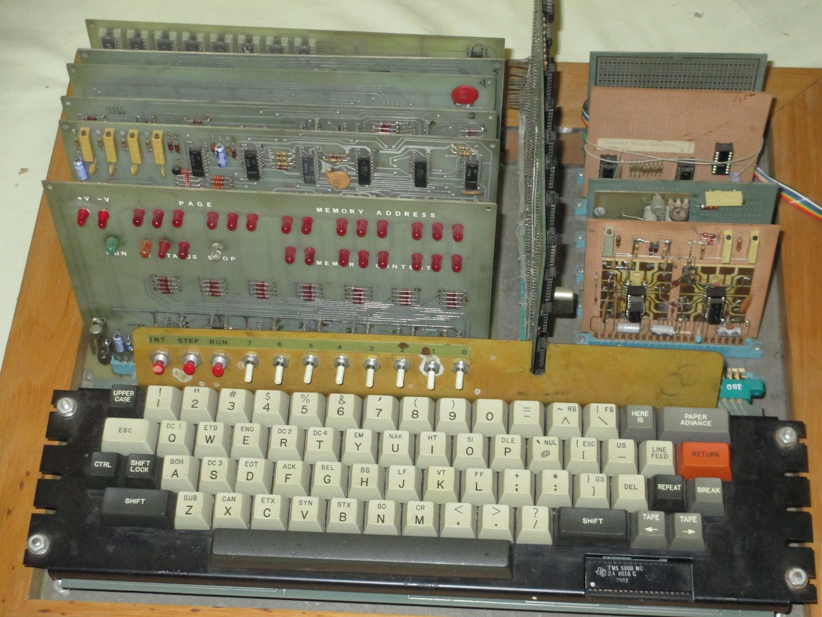
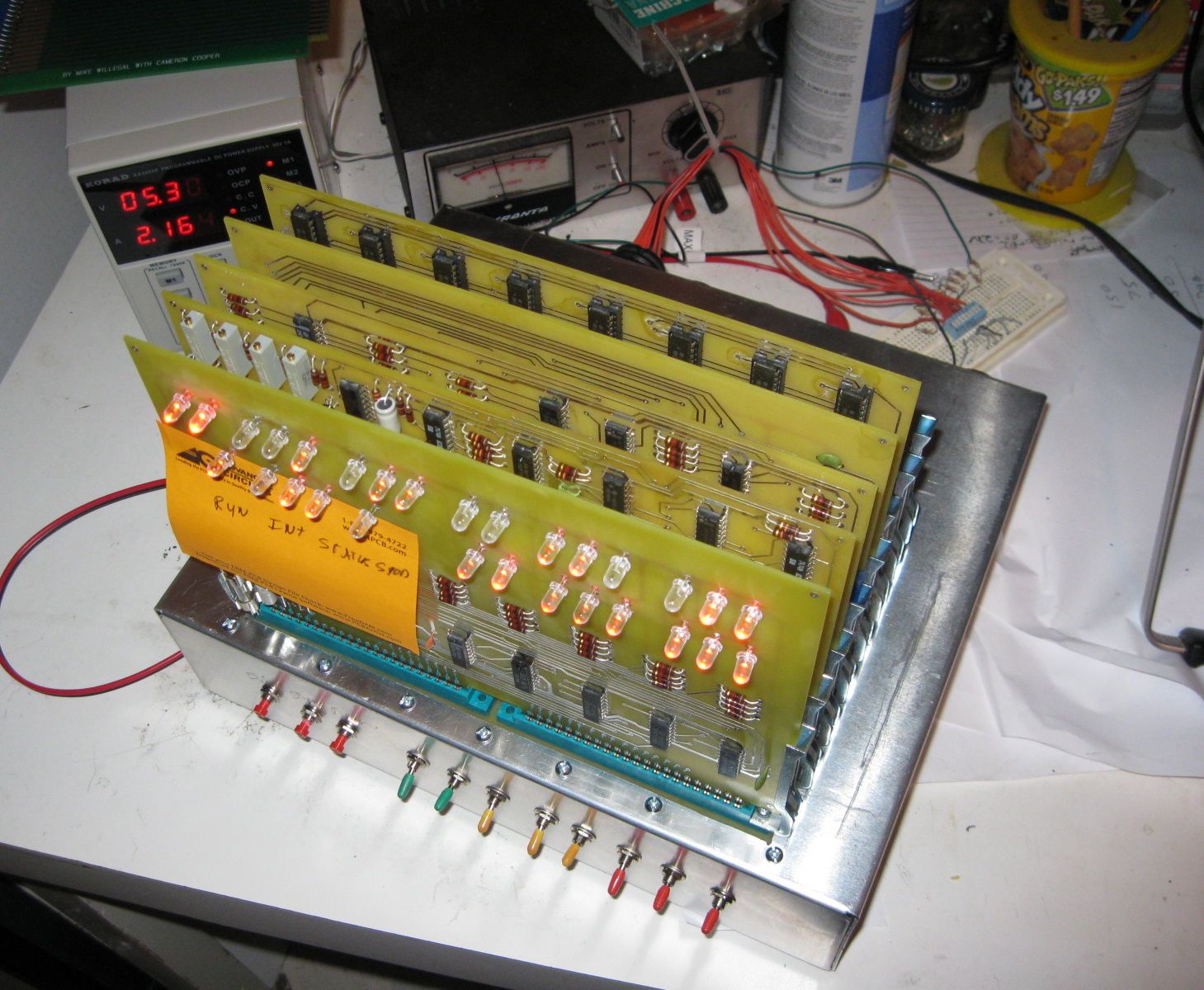
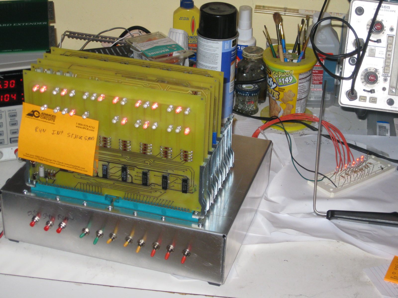
One of the challenges of working with the SCELBI 8H, which doesn’t have a built in monitor, is loading software.

To address this, I have written a minimal serial boot loader that can receive serial data and write to memory. It takes a few minutes to toggle in the thirty-seven bytes, but it should save plenty of time, compared to toggling in an entire practical program. In the days of the SCELBI, the most common serial device was a TTY, that could dump data from paper tape at 110 baud using a current loop interface. This loader has it’s timing loops configured to receive 8 bit data at 2400 baud, but some hobbyist may want to retime to run at a TTY’s 110 baud.

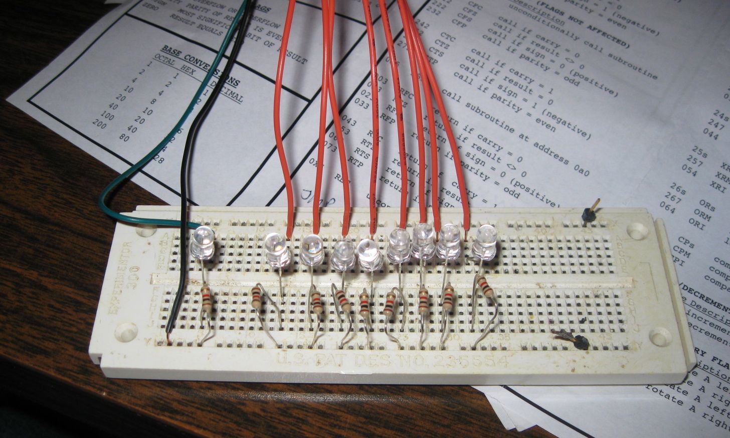
This loader will work with a current loop or RS232 interface, depending upon what is connected to the TTL input port 5, bit 8. In my case, I connected a TTL to RS232 dongle that I had built for another task. This dongle is very simple. It consists of a MAX202 chip, some capacitors and some connectors. The other side of the dongle is connected to a modern PC, which can be used as a terminal and a source for dumping data to the SCELBI. Eventually I plan on building reproduction SCELBI current loop boards for those that want to interface to a TTY or other current loop device.

This loader is assembled to run from location zero, but it would be trivial to move it elsewhere.

Here is the listing for the minimal loader.


INPUT:
000:113 INP INPORT
001:240 NDA ; check start bit
002:160 000 000 JTS INPUT
005:026 010 LCI 8
TIMER: ; 1 1/2 bit times
007:021 DCC
010:110 007 000 JFZ TIMER
013:036 010 LDI 8 ; grab 8 bits
DATAIN: ; get 1 bit
015:113 INP INPORT
016:022 RAL ; move to carry
017:301 LAB ; fetch current byte
020:032 RAR ; shift in this bit
021:310 LBA ; save in B
022:026 003 LCI 3 ; delay 1 bit time
BITTMR:
024:021 DCC
025:110 024 000 JFZ BITTMR
030:031 DCD ; 8 bits captured?
031:110 015 000 JFZ DATAIN ; no, continue
034:371 LMB ; store byte
035:060 INL ; increment pointer
036:110 000 000 JFZ INPUT ; wrap?
041:050 INH ; increment MSB
042:104 000 000 JMP INPUT ; continue

Here are the instructions:

  • Toggle in program with front panel
  • Set source to 2400, 8 bits, no parity
  • Set H and L with panel to start addr
  • Set PC to 0
  • Run
  • Send data from source
  • Interrupt when data has been sent
  • Decrement address
  • Using panel, check last byte with LAM
  • In the next few days I’ll put together “put char” and a “get char” routines that will also run over the 2400 baud, 8 bit interface. These will be used as the I/O drivers for downloaded apps, and should be combined with any app that is to be downloaded.

    One last thing. The SCELBI is very tolerant of CPU clock speeds, but for this loader to work correctly, the CPU clock has to be very close to 500KHZ. If your recieved data is garbled, there is a good chance your CPU clock is not correct.

    SCELBI Base PCB Checkout Complete – If You Were Not Part of the Early Adopter Program, You Can Order Your Board Sets Now

    With I/O testing complete, I can’t think of any other tests to run and I declare testing of the 6 SCELBI 8H reproduction PCBs, complete.

    The only issue found in this set of boards, is a minor issue with hole size for the Zener diodes as documented here.

    With the completion of testing, I’m opening regular ordering at a price of $300 for the six board set. For an extra $35, you can also order a D8008 processor (the 8008 is only available with board set orders).

    Please send an email to mike@willegal.net for detailed ordering information. As a bonus, while supplies last, I’ll throw in a scrap, non-functional, backplane PCB that can be used for backplane/chassis mock up work.

    Right now I’m limiting sales to 1 SRAM card (1K) per board set, but once I sell a few more board sets, I’ll get another batch of SRAM PCBs made, and open up SRAM PCB sales independant of the board sets.

    Card Guide Caution

    The traces on many of the SCELBI PCBs travel very close to the edge of the board and the card guides. Since the boards do not have a solder mask, it is possible that one of these traces could short out with the metal card guides. Though the card guides are not electrically connected to anywhere else, this potential for accidental shorts should be avoided. After inserting the cards, I carefully checked for shorts. The only card that has a trace actually touching a card guide, is the input card. To prevent accidental shorts I insulated this connection with masking tape, as shown here.

    Input Card Potential Short

    Input Card Potential Short

    I also checked to make sure that I hadn’t made a mistake in my layout, but the original cards also appear to have this potential issue. See this crop of the image of an original input card from http://www.olson-ndt.com/Scelbi/

    Input Card Right Edge

    Input Card Right Edge

    Input Port Testing Also Successful

    The six input ports on the SCELBI each have an independent 8 bit data bus that is not connected to anywhere else, except that ports dedicated input circuit. Like the output ports, the input ports are also implemented using 78S11 sockets and 86CP11 plugs. The sockets contain 1 ground wire at pin 11 and 8 data wires from pins 1 through 8. There is nothing connected to pins 9 and 10.

    Since 9 is not connected, I decided to reuse the test cable I made for output port tested, except change around the breadboard to control input lines, instead of monitor output lines with LEDS.

    Input Port Test Rig

    Input Port Test Rig

    In this case I connected the 8 data lines to 1K ohms pulled up to 5 volts. Since 5 volts doesn’t exist on the cable, I wired the 5 volts from my 5 volt power supply. Using a series of 8 DIP switches I could connect any one of these lines to ground, as I pleased.

    Now I basically repeated what I did for the output port test, only using the INPUT instruction and dumping the contents of the accumulator to memory to verify that the read was successful.

    Input Port Test

    Input Port Test

    Note that after running this test, I realized that the input signals are already pulled up on the input board, so the pullups in the test rig aren’t actually necessary.

    Output Port Testing Successful

    The SCELBI has 8 output ports. Each port is implemented with an Amphehol 11 pin 78S11 female socket. The sockets are still available, but tend to be expensive, often $12 or $13 dollars or more. Each port is connected to the SCELBI 8 bit data bus (pins 1-8), system ground (pin 11) and a strobe signal (pin 9). Pin 10 is left unconnected.

    The 8 bit data bus, as the name suggests is bussed across all 8 output ports and to the rest of the computer. The ground is also connected to the backplane system ground. The strobes are unique for each port. This is, in fact the only difference between each output port. Output hardware must latch the data bus when the strobe signal is seen on that port.

    The mating plug is another expensive connector, called an 86CP11. Here are front and back images of an 86CP11.

    front 86CP11 plug

    front 86CP11 plug

    Back 86CP11 Plug

    Back 86CP11 Plug

    It took me a while to figure out how to solder wires to this connector. I used 22 gauge solid conductor hook up wire. You strip about 3/8″ from one end (give or take) and stick the wire into the tip from the back of the connector until the conductor comes out the little hole at the end of the tip. I then bent the conductor over a bit so it wouldn’t slip back in and soldered from the tip of the plug. Then I carefully cut the excess conductor off. I’m sure some old hand will send me an email, saying how I’m doing it all wrong, but it worked for me.

    I didn’t have 10 different colors of wire, so I used black for ground, red for the 8 data lines and green for the strobe.

    For output port testing purposes, I connected the other end of the wires to breadboard. Each wire was connected to a LED which was connected to ground through a 1K resistor.

    Output Port Test Rig

    Output Port Test Rig

    Now by writing data to the output port, I visually check each line, including the strobe, by executing simple code fragments. I plugged the test rig into port 0 and powered up the SCELBI. I loaded this simple code fragment into memory, starting at location 0.

    OUT 0
    JMP 0

    Next I manually loaded the accumulator with the data I wanted to write by jamming in a LAI instruction and then jammed a JMP 0 instruction. I then stepped through the little loop, watching the LEDs on the test fixture. I then tried a few other data patterns by putting different patterns in the Accumulator and rerunning the test. Then I moved the connector to the next output port and loaded location zero with the OUT 1 instruction. I repeated the test for this port and the remaining output ports.

    Output Port Test

    Output Port Test

    Everything checked out perfectly and I’m declaring the output port logic in perfect working order.

    SCELBI CHASSIS

    First a look at the back of the chassis with the 78S11 sockets mounted. I don’t have the 86CP4 power socket installed. That will come later.

    Chassis with 78S11 Sockets

    Chassis with 78S11 Sockets

    Now a view of the completed I/O wiring.

    Chassis I/O Wiring

    Chassis I/O Wiring

    This is a lot of work. A ground wire is connected to pin 11 of each port. This is 14 wires.

    The output ports have 8 bits bussed directly from the data bus that goes to the SRAM slots to all the sockets. Plus another strobe line is connected for each port from the DBB card. I imagine any output device would be designed to latch output data when it sees the strobe for the connected port. This is 8×8 + 8 or 72 wires

    The input ports have 8 bits of data connected separately for each port directly to the input card. This is 8×6 or 48 wires.

    Total number of wires 14+72+48 = 134 wires. I have noticed that at least one original SCELBI had only the first two input ports wired. I’m guessing the builder thought that two would be enough for now, and if he needed more, he could add them later.

    How to Make the 78S11 Cutouts in the Back of the SCELBI

    Nothing about the SCELBI is straight forward. The cutouts on the back of the chassis for the 78S type connectors is another example of this.

    I puzzled over how to cleanly accomplish this for quite a few hours. Note that the power connector is a 86CP4 plug, so we are talking about 14 holes for the I/O ports and 1 hole for the power connector for a total of 15 holes.

    Back Chassis Cutouts

    Back Chassis Cutouts

    After much research, I finally happened upon a tool that was expressly designed to punch out these holes. The solution is a tool made by Greenlee called a radio chassis punch. The size you need for 78S type sockets is the type 732, sized 1 11/64″. They appear to sell pretty frequently for under $50 on ebay, but I happened to find a NOS one on a nearby distributers shelf for under $25.

    Here are some example holes made by the punch. There is a 78S socket in one hole and the punch in another. You need to drill a 1/2 inch pilot hole before you can punch out the final hole with this tool.

    Trial Punch Holes

    Trial Punch Holes

    One thing I did to make punching out my chassis more accurate, was to create a pattern based on a 12″ by 3″ chassis back panel. I determined that the spacing between the 1 1/4″ diameter connectors is only 1/8″, so your layout has to be pretty accurate. My BUD AC413 chassis is only 3″ high, so you will have to adjust vertical dimensions a bit for a SCELBI 3.5″ high chassis.

    Back Chassis Pattern

    Back Chassis Pattern

    The next step is to install all those sockets and wire them up.

    SCELBI Memory Tests Pass in All Slots – I/O left to checkout

    I used the memory test in the user manual to test each page in each slot in the system and it appears fine. This test is pretty basic, but considering that it had to be toggled in each time I moved the memory card to a new slot, I’m considering it good enough. I did not check multiple memory cards together, but I’ll assume that Nat and others did that back in the “old days”.

    Power consumption for a fully populated memory card compared to only 1 bank (8 chips) populated is a little over 2 amps versus 1.5 amps on the 5 volt rail and a little over .5 amp versus .3 amp on -9 volt rail.

    I still need to checkout I/O ports and that may take a bit, as I still have to hand wire the chassis for the 78S11 connectors used for I/O.