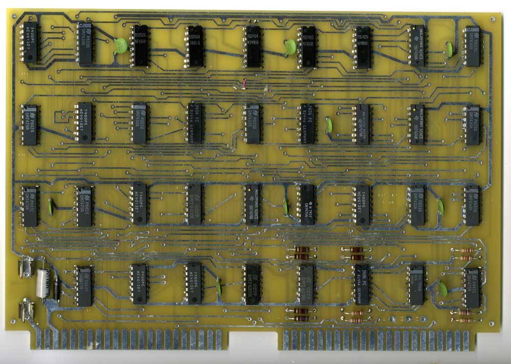
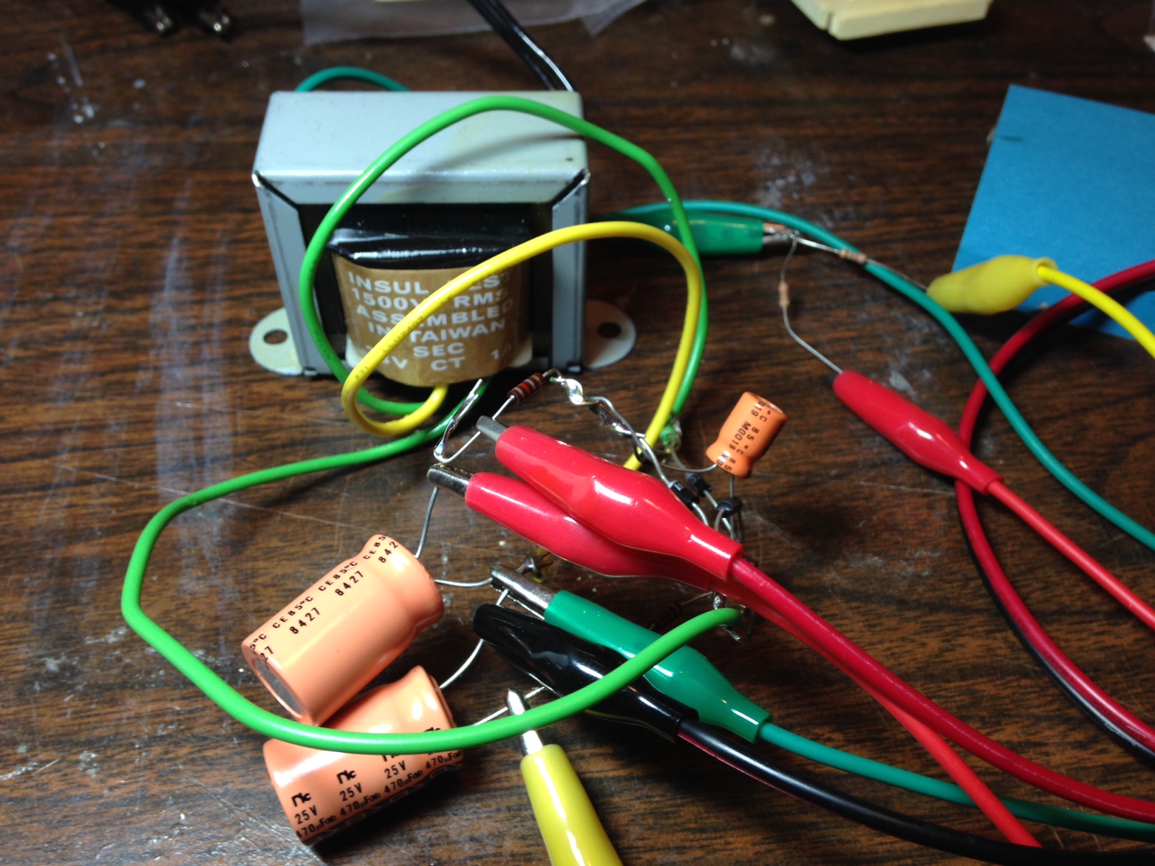
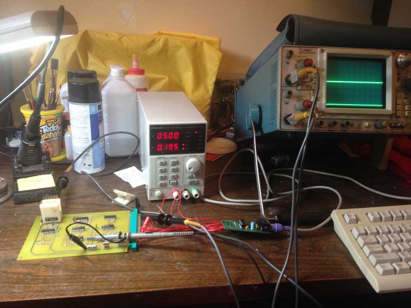
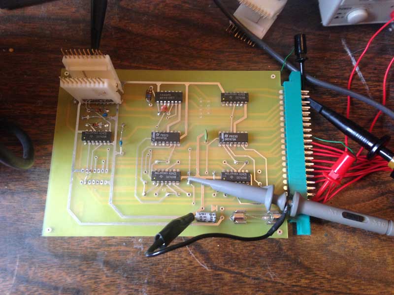
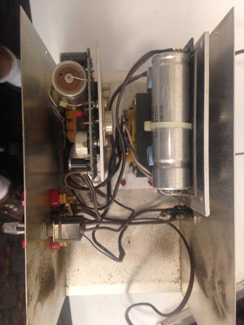
Before I finalize on values for the SCELBI scope analog supply components, I needed to know how much power the board consumes. To determine this, I set up two bench supplies to power the board and measure current consumption.
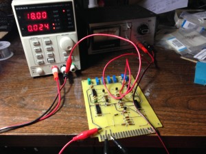
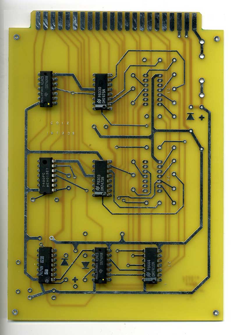
Scope Analog Board Current Test
Current consumption on both positive and negative rails measures at only about 25 mA. It’s possible current could vary a bit when hooked up to scope output and the digital board for input, but looking at the schematic makes me think that it’s not going to change very much.
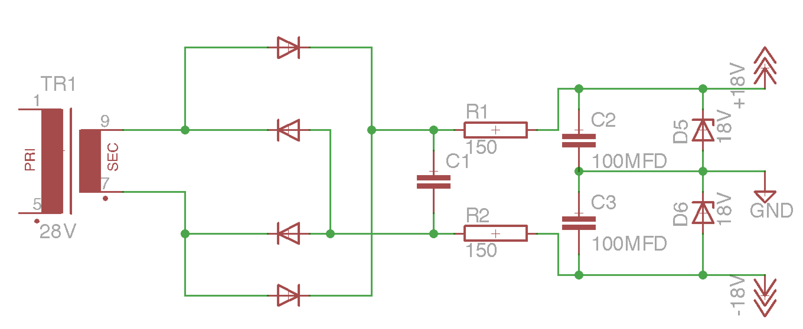
The way this zener based regulator works, is that if the voltage is over 18 volts, the zener shunts current to ground causing a voltage drop over the series resistor. The zener selected has to have enough current sinking capability to shunt the excess current to control the voltage. The resistor has to have enough current capacity to sustain the current for the entire circuit.
With the 28 volt transformer I found in my stash, the rectified DC voltage with no load is about 22 volts. The formula for finding the amount of current that the series resistor must handle is simply ohms law. Here is the formula for the 150 ohm resistor found on the original power supply.
I=V/R
V= 22-18
R=150
I= (22-18)/150
I = 4/150
I = .026 AMP
I = 26 mA
Here’s the tricky part. For a zener to regulate correctly, it must pass a minimum amount of current. The current, the series resistor passes, will be split between the zener and the board. If the board consumes 25 mA, then almost the entire drop of 26 mA over the series resistor is due to the board, not the zener and the zener will only be passing 1 mA. I checked the data sheet of a typical zener, the Fairchild BZX79C18 and it is specified at 5 mA. 1 mA may not be enough to regulate the voltage well, at least for that part. Either a larger input voltage coming from the transformer or smaller series resister will be required, if I was to use a BZX79C18.
If I switch to a 120 ohm series resistor. The formula looks a little more promising.
I = (22-18)/120 = .033 AMP
I = 33 mA
With the board consuming 25 mA, this leaves 8 mA for the zener to shunt, which should be enough, at least for the BZX79C18.
I don’t have the specification for the original power supply’s transformer, which may account for the slightly different series resistor value of 150 ohms that is in the original device.
The wattage capacity of the series resistor and the zener is also important. The formula for watts is simple W = I x V. First for the resistor.
W = I x V
W = .033 x 4
W = .132 watts
W = 132 mW
Assuming my other calculations and measurements are correct, even small .25 watt resistors should be sufficient for this application.
Then for the zener
I = .033 – .025 (the board consumes .025 Amps, which is not shunted through the zener)
I = .008
W = .008 x 18
W = .144 watts
W = 144 mW
The BZX79C18 is rated at 500 mW, so it also should be fine for this application.
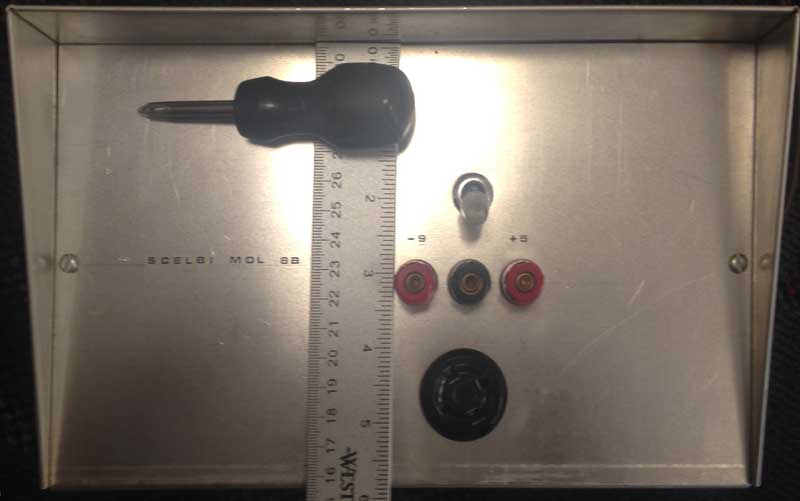
With the low current requirement for this power supply, I’m going to pick up a smaller transformer, as the 1 AMP transformer I had in my parts stash, is clearly overkill and will not fit in the oscilloscope interface enclosure.