
The release of a new version of my OS/X SCELBI/8008 emulator was motivated to provide support of the Modified Creed Monitor for the 8008. To do this, I added menu options to support to optionally setting (input) and clearing (output) the most significant bit of input and output serial data. For the MCMON, the input menu for set the bit should NOT be set. The output setting doesn’t matter.
Author Archives: Mike
8008 Mini Monitor and EPROM support for the SCELBI-8H
I just finished adding two new web pages to the 8008/SCELBI area of my website. Take a look, if you want to see what can be done with 256 bytes in an 8008 and how to add a monitor and EPROM to your SCELBI-8H.
SCELBI Main CPU/DBB/INPUT and Front Panel Boards restocked
I did add a silk screen/legend to the front panel. Some original boards had it, and some didn’t. I figured I’d add it on this batch.
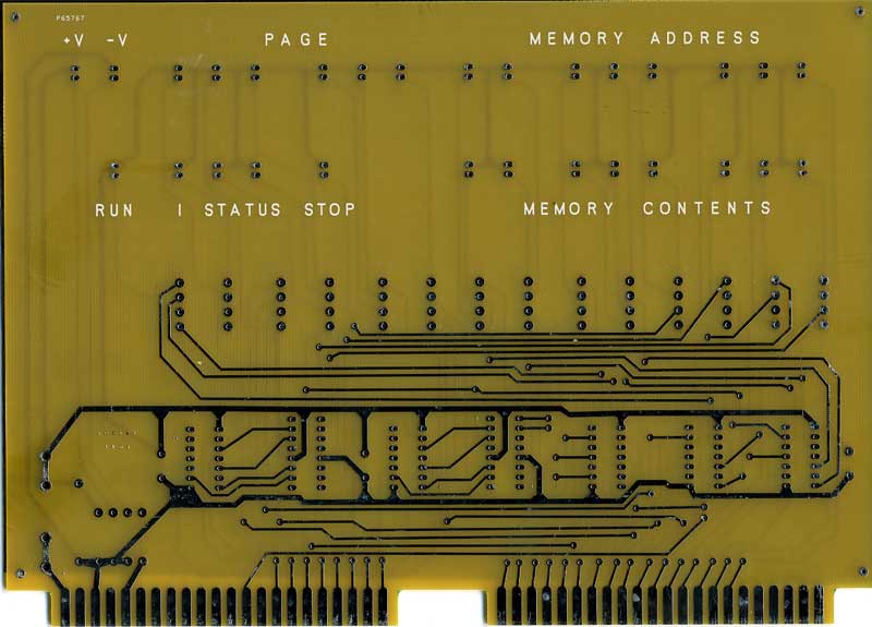
Front Panel with Legend
Only other difference from first batch is slightly large holes for Zener diodes.
Another SCELBI Cassette Write Board (with logic changes/fixes)
While working on the SCELBI cassette write board, I found some issues which were reported in this blog post. I found that I had detailed images of a second cassette write board, and it looks like the problems on that first board that I looked at, were corrected on the second board.
The first board is the one found at the CHM, and was photographed a while back by Jack Rubin. The serial numbers on the SCELBI associated with that unit are in the single digits, so that unit was apparently a very early unit. The second, corrected board, was part of the collection of Nat Wadsworth. I am only aware of one other cassette interface, but I don’t have images of that unit. I don’t know how many were made before the corrections were made.
Here are partial images of the front and back of relevant sections of both boards. Red arrows on images of the Nat Wadsworth unit show where visible changes were made.
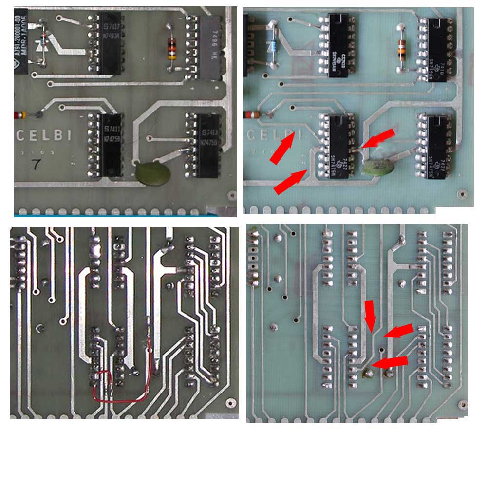
Cassette Write Board Changes
Note that the changes are somewhat different than the what was done in rework on the CHM unit. These changes don’t match the schematics, but I was able to piece together what was done and why.
First, let’s talk a bit about what is going on, by reviewing this section of the schematics.
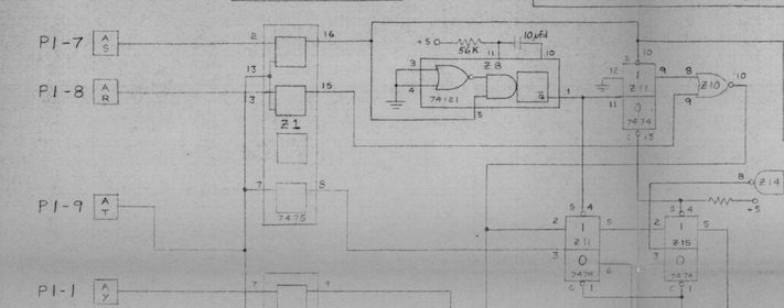
Cassette Schematics – Z1
The chip associated with all these changes is a 7475, a part that has 4 bi-stable latches. Here is the key part of the data sheet – the truth table and the pinout.
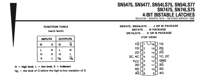
7475 Data Sheet
The function of this chip is pretty simple. Whenever clock input 13 is high, the chip’s output pins, 16 and 15 follow the input on pins 2 and 3, respecitively. Also, output pins 10 and 9 follow inputs 6 and 7, respectively, when clock input 4 is high. When inputs 4 or 13 go low, the associated pair of outputs, are “frozen” or are “latched” into their current state at the time the clocks inputs go low. Note that there are normal and inverted outputs for each latch.
In the schematics, three inputs are connected from a SCELBI output port to this chip. There are two data bits and the port’s output strobe. The output strobe is a high going pulse that occurs when an 8008 OUT instruction addressed to this port. The data bits are connected to the SCELBI write data bus, so will change rapidly, as the 8008 writes to memory or output ports. The strobe is connected to the clock input (pin 13) of the 7475 latches 1 and 2. This circuit allows the 7475 chip to capture 2 bits of the SCELBI output data onto latches 1 and 2 whenever an out instruction is directed to the output port connected to the cassette interface.
What about the two other latches of the 7475? In the schematics, the clock (on pin 4) for outputs 3 and 4 is not connected. What usually happens on unconnected inputs of 74XX series logic is that the input will “float” high. As mentioned before, if the clock inputs are high on the 7475, then the outputs will simply track the state of the inputs. The 3rd latch of this chip is not connected or used. However the 4th latch (pin 7) is connected to the strobe input, so the output will follow the strobe all the time. The inverted output on pin 8 is used as a clock elsewhere on the board. The function is a buffer and inverter of the strobe input to the board. Note that letting an input “float” high is not a good design practice and it’s possible that clock input on pin 4 was directly tied to +5 volts, which is connected to pin 5. It is not connected on the bottom of the board, but could be connected on the top of the board, which is obscured by the chip. The only way to know for sure, would be to use an ohm meter to determine if pin 4 is connected somewhere by a trace that is obscured by the chip. I don’t presently have access to this board, which is in storage at the CHM, so I can’t do this. My best guess, based on the extensive use of pull up’s elsewhere on the SCEBLI boards, and lack of a connection in the schematics, is that it was left to float high and was not connected.
As mentioned in the previous blog post, the first version of the layout has two significant problems.
1) The strobe output wasn’t connected to pin 7 of the 7475. This is rectified with a jumper wire.
2) The output on pin 8 (which is the inverted strobe signal), is not correctly connected to the rest of the circuit. This is rectified by a cut and jumper as can be seen in the image of the back of the board.
So what did the people at SCELBI do, to fix the problems in revised layout.
1) Power and ground connections to the chip were rerouted to make room for signal traces that needed to be added.
2) The inverted strobe output which was supposed to be on pin 8 was moved to pin 11, which is the inverted latch 3 output. This was done to make it easier to connect to the rest of the circuit. It was also disconnected from the strobe input connection.
3) The floating clock input on pin 4 was tied to an existing pull up resistor.
4) The latch 3 input was connected to strobe input by running a trace under the chip to pin 13, which was already connected to strobe. I actually can’t verify this change, but I can be fairly certain that it exists, since the circuit would not work without this trace.
Note that this change to use latch 3 instead of latch 4 for buffering and inverting the strobe is not reflected in any schematics that I have seen. The schematics actually don’t match either of the boards described in this description.
If you look at CAD images of this section of the board, you can see how the changes were made. Blue traces are on the bottom layer and red traces are on the top layer of the PCB.
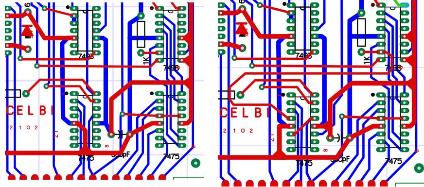
Write Board Changes
I have repeated this sort of exercise numberous times over the years to solve various inconsistencies in schematics and PCB layouts in a number of vintage computers. Understanding a vintage design frequently requires detailed detective work, but with time and patience, most mysteries can be solved.
One last comment about the nature of the problems with this board. Of the thirteen SCELBI boards that I have investigated in detail, this is the first significant layout problem I have run across. There is an issue on the DBB board with a single missing trace. In this case, the connections to the 7475 were botched and had to be redone. This is a very unusual and unexpected mistake from the engineers at SCELBI.
Cassette Write Board Rework
More progress on the SCELBI cassette write board. I have figured out the reason for the rework seen on at least one board.
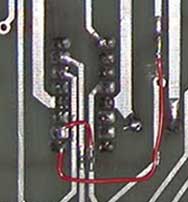
Cassette Write Board Rework
There are two wires and a cut on this board. In both these cases, the PCB didn’t follow the schematics. Both changes are related to chip Z1 connections.
In case 1, pin Z1-7 should have been connected to Port A, pin T. Port A, pin T is already correctly connected to Z1-13 and Z2-13 and Z2-4. I’m not sure if this omission was on purpose or not. Routing to Z1, pin 7 would require running a trace on the top of board, from Z1-13 out the top of Z1 around the outside of Z1 to Z1-7. This would also require re-routing a couple of other traces on the top side of the board to make room for this new trace. It’s very unlikely, but possible the layout person didn’t want to mess with this and decided to just require the board builder to add a wire.
In the second case, Z1-8 is not connected to Z11-3. Instead Z11-3 is connected to Port A, pin T. The fix requires cutting the trace from Port A, pin T, after it splits and runs through a via to go to Z2. Then a wire can be soldered from the cut trace to Z1-8. This is clearly a layout error.
I still have at least one more mystery to solve on the cassette write board, before I’m done with it, but the layout is shaping up real well.
Economics of Selling Vintage Computers/Kits/Components
In March of 2011, on the MARCH Yahoo Forum, I suggested that having a PCB fab build a batch of reproduction boards for the MARK-8 would cost a small fortune.
Perhaps I should follow my own advice. In Feburary of 2013, I invested a small fortune in a similar project, the SCELBI-8H. It has taken over 2 years to sell 19 pcb sets for the SCELBI-8H and SCELBI-8B. I’ve kept track of my investment in PCBs, as well as all the other components and materials that it took to build a working example of each system. Despite selling individual boards for a profit over their cost, I can honestly report that the overall project has cost me a significant amount of money. Now this investment has been worth every cent, but almost entirely due to the fun that I’ve had and friends that I’ve made, not due to any financial reward.
Now it’s possible that after a few more years of selling SCELBI PCBs, I’ll have managed to break even on the project, but it will always be a work of passion, not profit.
Many retro products only come to the market for a short period of time and then disappear. I believe that this is due to the tiny market and low profit realized. Once you have built something, the excitement of creation is replaced by the routine work of handling inquiries, ordering parts, packing, shipping products and supporting customers. If you are only making a few dollars and would rather be spending your spare time on a new project, it is easy to see why new batches are not made once inventory is sold off. It wouldn’t surprise me that some products are pulled off the market, even when the inventory still exists, just because the developer just doesn’t want to deal with the hassle.
There are a few products that seem to have defied the odds – but they are very few in number. An example is the series of CFFA cards for the Apple ][ computer. Rich Dreher routinely makes and sells batches of hundreds of them. The numbers of units he sells, absolutely amaze me. He also has an Apple 1 version of this card, but according to his web site, it appears that he has only sold a little over half of a batch of 200 that were made two years ago. I wonder if he will make another batch of the Apple 1 version, when the current batch is finally sold. Vince Briel has had some very good success with his vintage work-alike kits, but I don’t think it’s enough for him to live on. Just doing a little basic math shows how how many would need to be sold to make a living at it. A Replica 1 kit currently lists for $149. Assume that you could make $75 per kit after costs. Then, assume you needed a $100,000 annual income, which is a fairly low income for an experienced engineer. Then divide the annual income requirement by the $75 revenue from each kit. The result would be a minimum of 1333 kits sold. Then, keep in mind that you would have to do that year after year in order to sustain a business. I just don’t think that the market is that large. In fact, Frank Achatz had a similar product to the Replica-1 on the market for a while called the A-ONE. It appears that he quit selling them and closed down his website a while back, which should tell you something about how difficult it is to either have fun or make a decent profit selling vintage kits.
New batch SCELBI FP, CPU, DBB & Input PCBs on order
I finally sold my 19th set of SCELBI boards. There were 20 sets made in the original batch for the 8H that were made in January of 2013. There were about an even number of 8H and 8B sets sold, and the boards I’m reordering are common between the sets, as I still have plenty of the boards that are unique to each system. There are only two differences between these new boards and the original set of boards.
1) The size of the holes for the zener diodes is being made a little bigger. Note that if you can find them, the leads for the original style zeners in the cans will fit in the original holes, but more modern zeners have thicker leads may not. Older boards will work fine with the more modern zeners, but the holes will have to be reamed out a bit and the leads soldered on both sides of the PCB.
2) This time around, I’m adding a silkscreened legend on the front panel board. The original SCELBI front panel boards came both with and without the legend, but I see more original units with the legend. This is why I’m adding the legend to this batch. When I made the first set, I thought that only early boards that were made before the advent of the aluminum front bezel had the legend. Later on, I discovered that a number of systems with the front bezel, also had a front panel board with a legend silk-screened onto it.
Radio Teletype Explored – part 1
Before I acquired Chris Galfo’s HAM software package for the Apple II, I had already developed a simple RTTY (Radio Teletype) setup that used my Apple IIe as a terminal. This series of posts will go over what I did to put together this setup. Before going into details of each component, I’ll go over the general setup and a few of the decisions that lead to the choice of major components.
In the beginning, my goal was to set up a RTTY station using 70’s era components. As you will see, I went a little into the 80’s in the choice of some specific components, but the basic platforms on which those components were based, were all available in the 70’s.
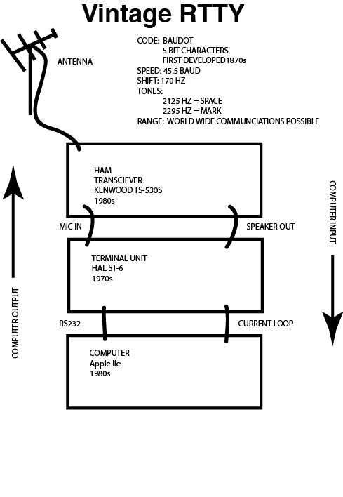
RTTY Block Diagram
As you can see, my setup is made up of 4 main components.
VCF east, Apple Monitor II Problem Explored
My setup at VCF east X had three monitors/CRTs setup as displays. They run all day, starting at about 9:00 AM, until the exhibit closes. One of them was an Apple Monitor II.
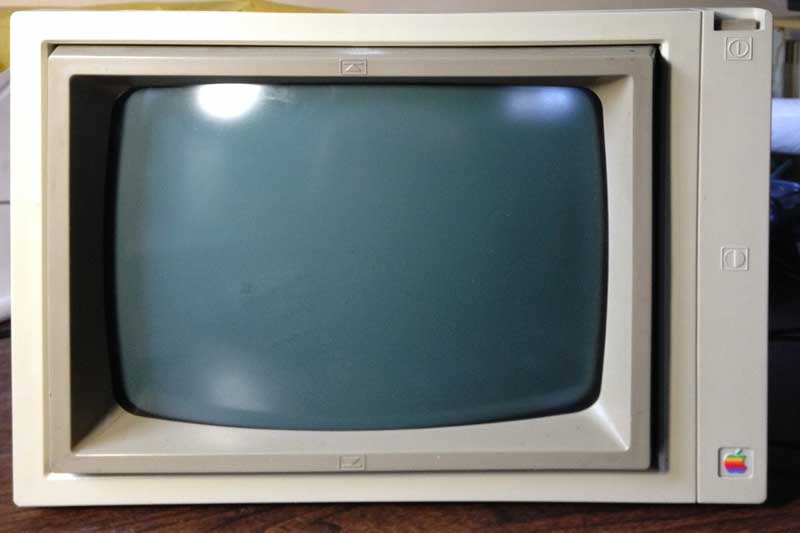
Apple Monitor II
Saturday, towards the end of the day, I noticed that the Monitor II wasn’t displaying anything and the “power” light wasn’t lit. Doing a quick check of power cords and trying a power cycle got no response. Since I was so busy, I decided to put it aside and remove one of the less important systems from my exhibit.
During day on Sunday, I casually asked Ian Primus, who is a CRT repair guru, if he knew of any common problems with the Apple Monitor II. He said that they never fail, but he’d be glad to take a look, later on. Late in the afternoon on Sunday, when activity was dying down, I decided to open it up and see if anything was obviously wrong. Once I got it open, Ian and Jeff Golas who was in the next “booth”, did a 5 minute investigation. They found that the fuse was blown, but little else obviously wrong. There was no obviously blown caps. Ian checked the rectifier diodes and a couple of power transistors, but they all checked out. Jeff measured the power consumption by using his meter as a jumper over the blown fuse, and it came out at .4 amps. Jeff said that he had a similar problem with one of his Apple Monitor II’s. It also blew the fuse. However his unit only measured .2 AMPS. With the quick inspection over, I closed it back up and decided to do a complete inspection when I got home.
I found some time Thursday night and took it apart for a complete inspection. After carefully making sure the tube was discharged, I disconnected the connectors going to the main logic board so I could pull it out enough to get to the back of the PCB. I set up my home-brew ESR tester and checked all the caps and could find no fault. I did find one located next to the horizontal output transistor heat sink that was a bit brown. However, it checked out fine, just like all the others. I also used my diode checker to check all the diodes and transistors on the board. I could find no fault with any of them.
After a few hours of probing, I was coming up with nothing, all the components that I could test, looked good. The next day, I stopped at a local shop to see if they had a replacement for the cap that was slightly brown, but they didn’t have the correct value. I decided that since it tested good, that I would leave it alone. I decided to clean the tarnished pins on the CRT yolk, reassemble and repeat the power test that Jeff had executed at VCF east. This time, the power consumption was down to .2 AMPs. I’m not sure why it dropped in half, maybe some connector wasn’t making good contact. Since the monitor is rated at 30 watts, .2 AMPs seems like normal power draw and matches what Jeff measured on his unit.
At this point, I was at a loss and decided to replace the 500 milliamp fuse and operate the monitor for a while. I figured that if there was something seriously wrong, the fuse would go again, or perhaps a marginal part would fail completely. I put everything back together and ran the unit for about an hour and it performed as designed.
I’m not sure if it’s fully repaired. I did find a SAMs repair manual for the unit online, which showed details of signals on the logic board, but since it’s working so well, I decided not to pursue evaluating all the signals in minute detail. For now, I just plan to keep a close eye on it whenever I am using it.
First of my “Vintage Digital Radio” Webpages is Up
This is the first of several webpages that I plan on putting up to document my efforts to integrate vintage computer operation with present day HAM activities. It is not currently linked to from my main homepage or other vintage web pages.
This page provides access to one of the first commercial HAM communications packages to be released anywhere. During my explorations of HAM integration with early vintage computers, I ran across several references to a software program released by a CH Galfo. Though I couldn’t find any actual images of the software or documentation, I was lucky enough to make contact with Dr Galfo, himself. Better yet, he was friendly and willing to help make the software accessible to vintage computer people. He sent me a floppy and a hard copy of the documentation, both of which I’ve been able to copy into a web friendly format. Dr Galfo indicated that since there is no commercial value, that you should feel free to copy and distribute.