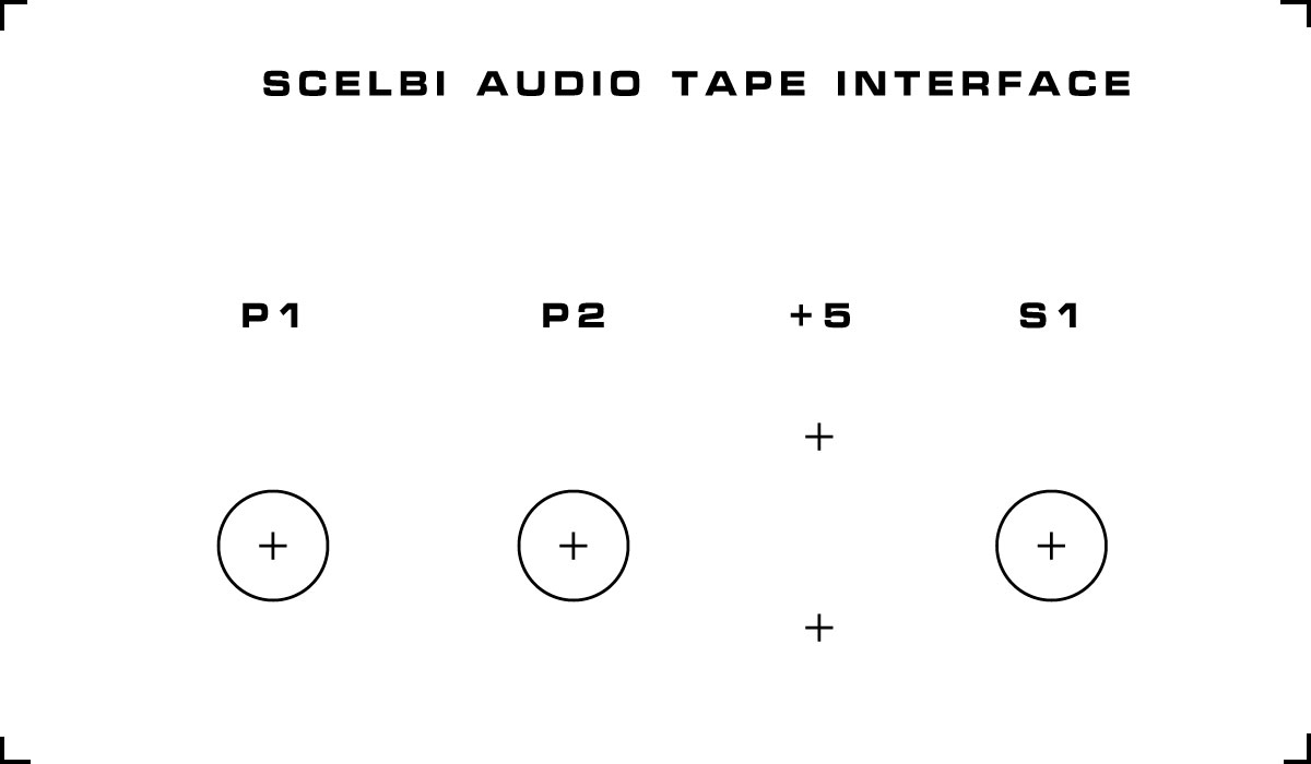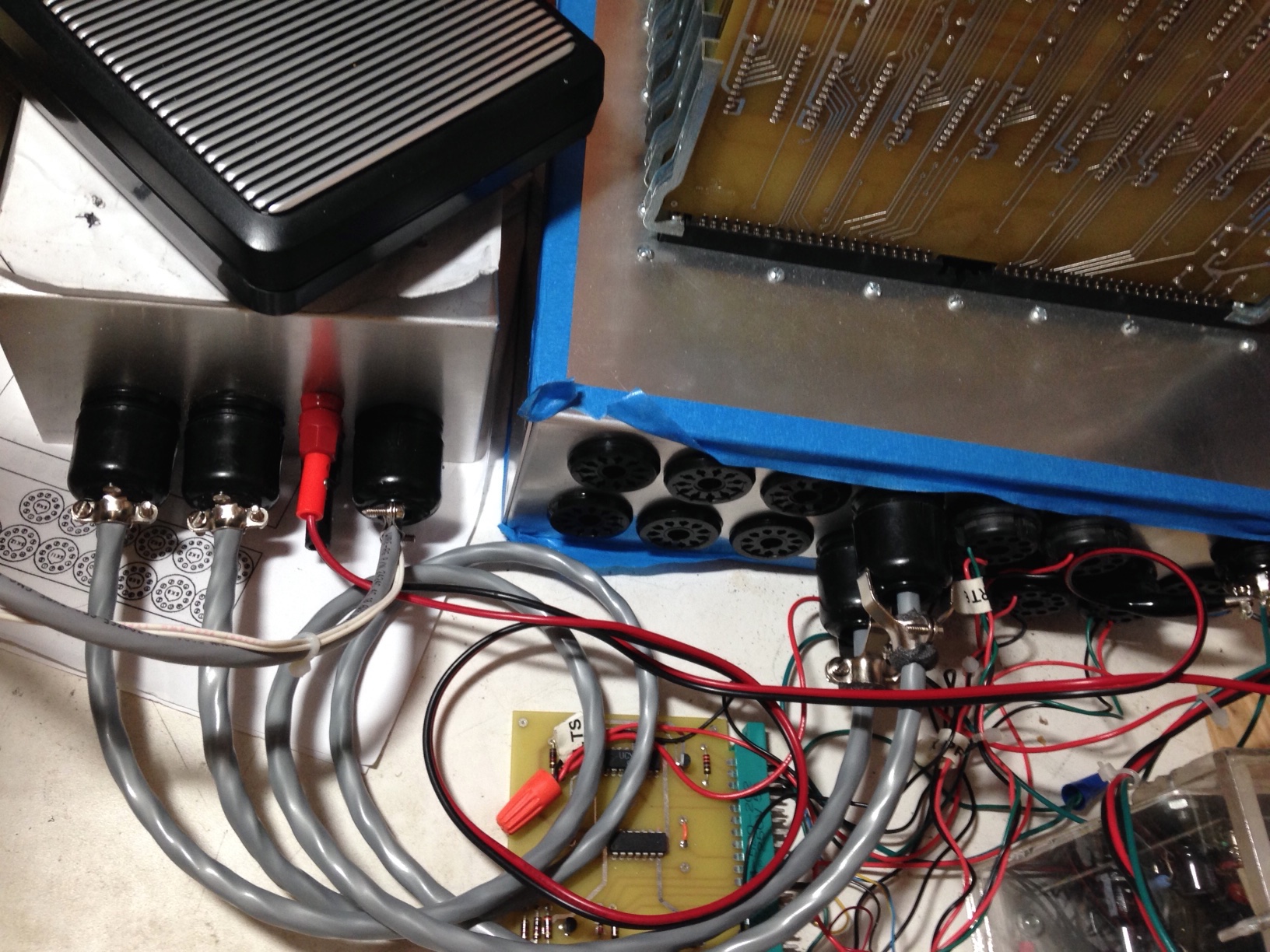
Cassette Interface Hooked Up
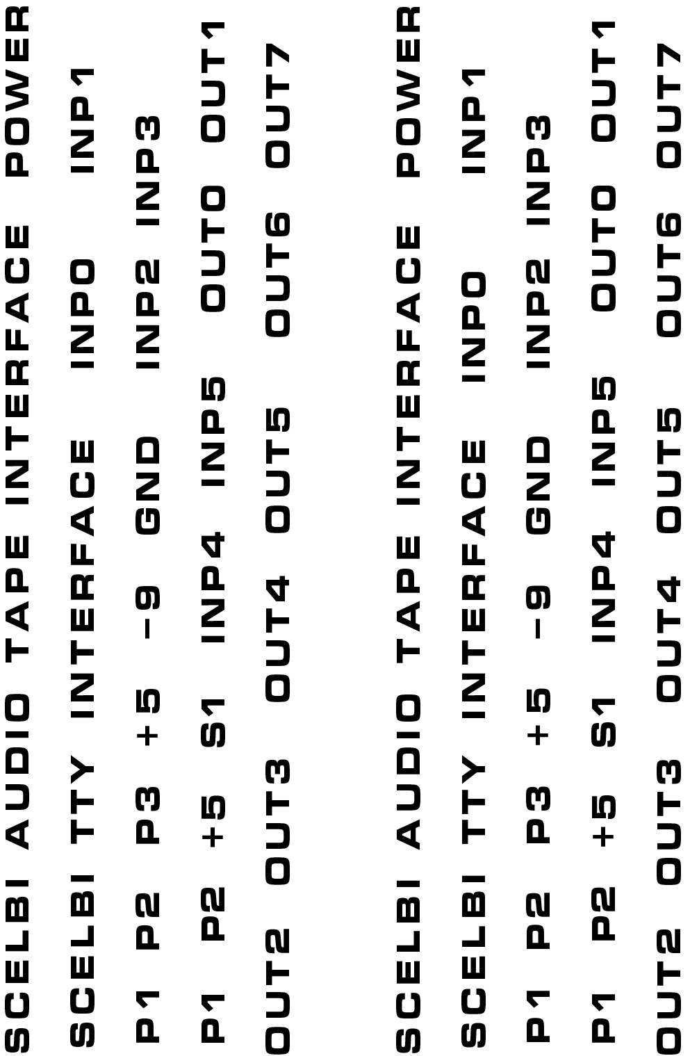
I have my reproduction cassette boards mounted in the enclosure and functioning. I still have the adjustment and read LED holes to drill and lettering to do. I have rub on lettering ordered and should have it in about a week. If it works out well, I’ll provide ordering information from the vendor, and you will be able to order directly from them. I made use of some white space and added lettering for keyboard interface, power supply and oscilliscope interface to the sheet.
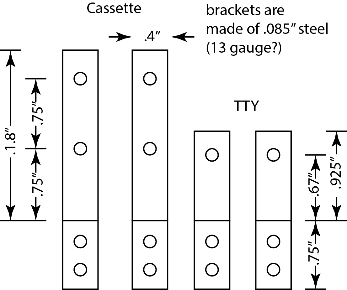
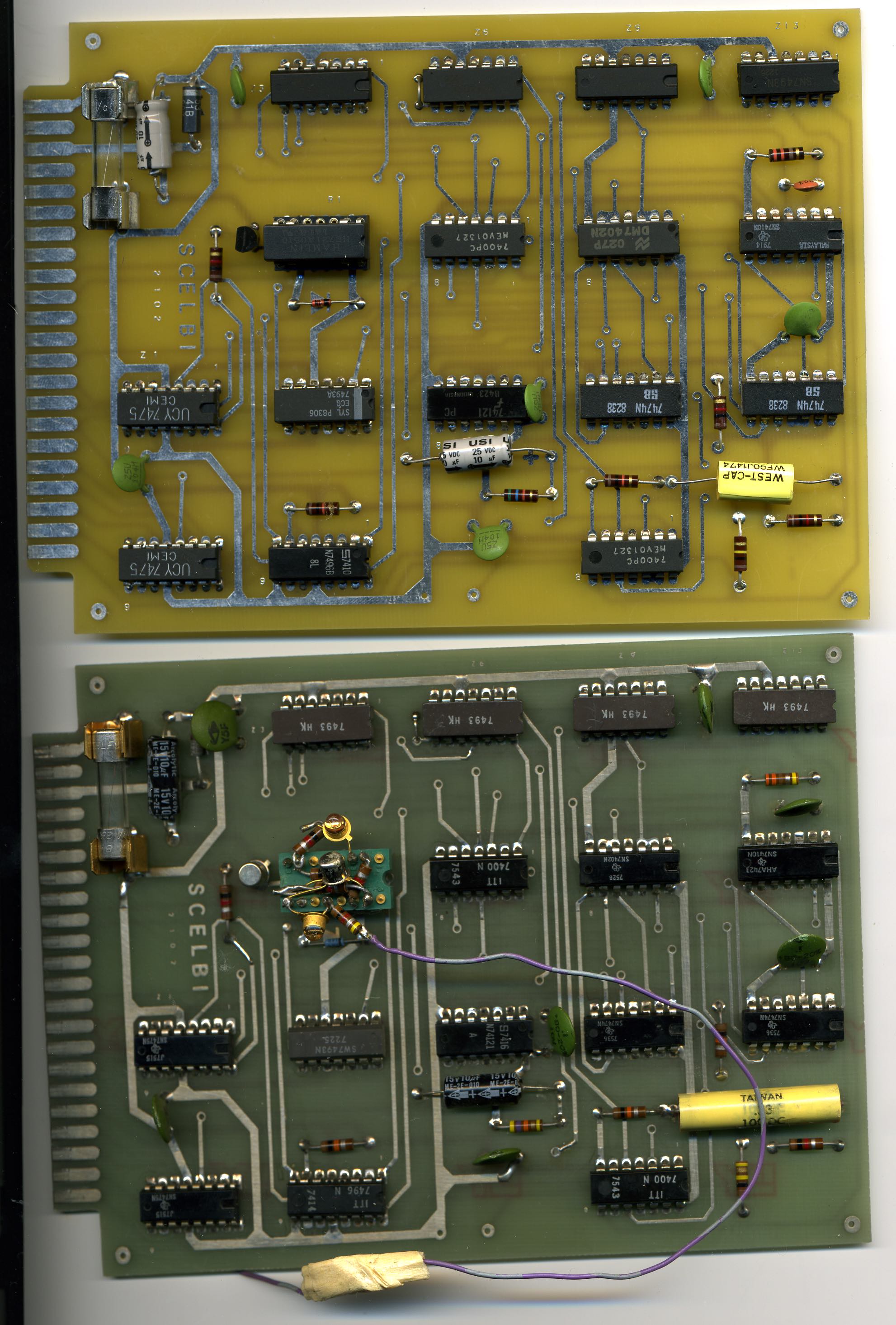
A couple of hints on construction/assembly and wiring of the cassette chassis. The brackets are mounted about 2/3″ back from the end of the chassis. It’s a pretty tight fit in there. Mount the edge connectors on the brackets, but don’t connect the brackets to the chassis. Connect wires to the edge connectors. Then feed the wires through the holes in the panel and cut to length and solder to the connectors. Power and ground lines all go to the power and ground connections on the edge connectors. Power and ground of the two edge connectors are bussed together.
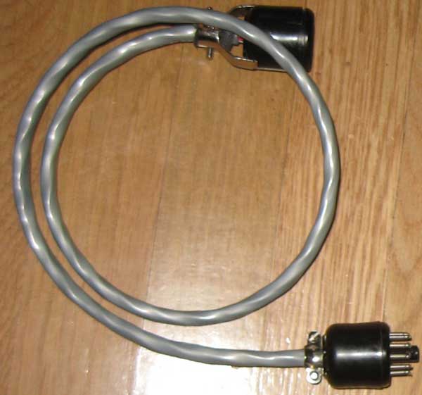
The cable to the cassette tape recorder is only four wires. They are write, read, and two ground wires. Both ground wires connect to pin 11, read is pin 1 and write is pin 2. Tie-wrapped to the outside of this cable are the 2 wires for the motor on/off control. I think that SCELBI might have used the same 4 conductor cable that was normally used for connecting the power supply to the main chassis for this application.
I’m still working on perfecting my silk screen making technique for the front panel. I’m determined to get to the point where I can get near professional quality results. Unfortunately I still have some learning to do.