Apple 1 Registry Updated – One of Which May be Myth Destroying

This update is way past due, I had knowledge of some of the new units since last fall. Three new Apple 1’s are listed. The most interesting is number 1-0052,owned by James Coble. His story seems to shatter the myth that the Byte Shop, not Apple, added the serial numbers on the units in the first batch. There were some issues with that story before, but this information seems to completely shatter it. I have a sent a query out to some experts to see if they can comment on what James has to say. Stay tuned for an update.

Another interesting note is that the unit that was sold on ebay is reported to be going to Germany. The world-wide market for Apple 1 continues to be stronger than the domestic US market. I think the Ford Museum purchase might have been an anomaly.

Lastly, I’m pretty skeptical about the report from the bay area about an Apple 1 being given to a recycler. That unit is not going to get mention in the registry until far more concrete details (like a picture) are revealed.

Old School Engineering

I just viewed Dave Jone’s latest video blog about the Sony Walkman. For some reason, I decided to download the service manual and have a look. One thing that I immediately noticed, was the lettering on the schematic appears to be another example of Leroy Lettering.

This caused me to reflect a little bit about my first year or two of college and my first job in industry. Before discovering computer science, I started out in a mechanical engineering program. The first engineering oriented courses you took, were drafting courses. I had no trouble with perspective and different technical aspects of drawing. However, I really had trouble creating drawings that looked nice, clean and sharp. There was no mention of Leroy or any other mechanical lettering system, so we had to hand letter our work. To this day, I don’t have the hand of an artist, and I think that lack of natural artistic ability held me back in that program. The skill of an artist, developed or natural is something that is apparent in a well done engineering drawing or schematic.

In years gone by, many engineers would spend their workday at a drafting board. I started my first co-op engineering job, in the late 70’s. That first company that I worked for, still had a drafting department for creating PCB layouts, as well as an art department that did the artwork for manuals as well as marketing material. The “uniform” of many of the experienced engineers was a white shirt, dark pants, a dark tie and a pocket protector. Second level managers omitted the pocket protector and added a sport coat. It’s basically the look of the NASA mission control team for the Apollo program.

A few years later, in the early 80s, I remember going for a job interview at IBM’s small system division. That was the first home of the IBM PC which was located in Boca Raton, Florida. Almost all the engineers there still wore that “uniform”. I did see one guy wearing a colorful shirt and jeans. He stuck out like a sore thumb. The IBM employee that was with me at that moment, pointed him out, and said he didn’t really fit in to the culture.

How times have changed.

8B Assembly Manual Mistake Discovered, the hard way

I’ve started working on building up a second set of the “core” SCELBI boards. I call the boards that are shared between the SCELBI 8B and 8H, the “core” boards. These are the front panel, the cpu, the DBB, and the input boards. When I built my prototype 8B, I didn’t bother to make new “core” boards, I just borrowed them from my 8H. Now that I have a new set of the “core” PCBs in stock, I figured that I would make up a second set, so that I could run both the 8H and 8B at the same time.

As part of the building of these new boards, I figured I’d use the 8B manual that I am in the process of digitizing. Yesterday, after completing the front panel board, I discoved that all my LEDs were installed backwards. The manual states:

The anode of the L.E.D. (shorter lead) goes in the top most hole (furthest away from the card connector). The cathode of the L.E.D. (longer lead) goes in the bottom hole.

This is actually the reverse of how LEDs are made – the cathode has the shorter lead, not the anode. I didn’t encounter this issue when building the board for my 8H, because the 8H front panel instructions were written for the old style LEDs in the cans, so I had to figure out the right way to connect them without benefit of the SCELBI manual. You would think that with all the projects that I’ve done, that I would remember how LED’s are constructed and connected. However pinouts are the sorts of details that are easily found in reference material, so I don’t put any effort into memorizing pinouts of anything.

As far as the newly digitized manual goes, one of my intentions is to add content and clarification when it is missing, but maintain the “character” of the original manual. I think, in this case, I will correct the text and add a footnote that explains how the original manual was wrong.

Cassette Write Board Verification in Progress

Verifing the layout against schematics, is an important step in my reproduction process. My usual method of schematic/layout verification is to print a copy of the schematics then mark each trace as I verify the connection with a marker. This time I did it all digitally using photoshop as a replacement for the paper.

Tape Write Schematic Markup

Tape Write Schematic Markup

The blue layer notes omissions, corrections or clarifications to the schematics. Most of these are due to the mistakes made in the initial rev of the board, which were later corrected. The version of the schematics I have access to, does not have those changes incorporated into them.

During this process, I did find a number of traces that were hidden under chips. Omitting these traces is an easy mistake to make. I missed one of these on the memory expansion board. This time, I am reasonably sure that I found them all.

Dr. Galfo’s Integer BASIC Compiler

I just put up a web page with documentation and DSK images of Dr Galfo’s Integer BASIC Compiler (IBC). This compiler was used in development of some well known Apple II games. It runs around six times faster than WOZ’s BASIC interpreter, so it’s worth trying out. Compiling an Integer BASIC program is easy. You simply load the program in the standard Apple interpreter and then run the compiler. You will be prompted for a few options and then, after the compiler is run, are given the option of running the program.

New Version of SCELBI OS/X Emulator Released

The release of a new version of my OS/X SCELBI/8008 emulator was motivated to provide support of the Modified Creed Monitor for the 8008. To do this, I added menu options to support to optionally setting (input) and clearing (output) the most significant bit of input and output serial data. For the MCMON, the input menu for set the bit should NOT be set. The output setting doesn’t matter.

Another SCELBI Cassette Write Board (with logic changes/fixes)

While working on the SCELBI cassette write board, I found some issues which were reported in this blog post. I found that I had detailed images of a second cassette write board, and it looks like the problems on that first board that I looked at, were corrected on the second board.

The first board is the one found at the CHM, and was photographed a while back by Jack Rubin. The serial numbers on the SCELBI associated with that unit are in the single digits, so that unit was apparently a very early unit. The second, corrected board, was part of the collection of Nat Wadsworth. I am only aware of one other cassette interface, but I don’t have images of that unit. I don’t know how many were made before the corrections were made.

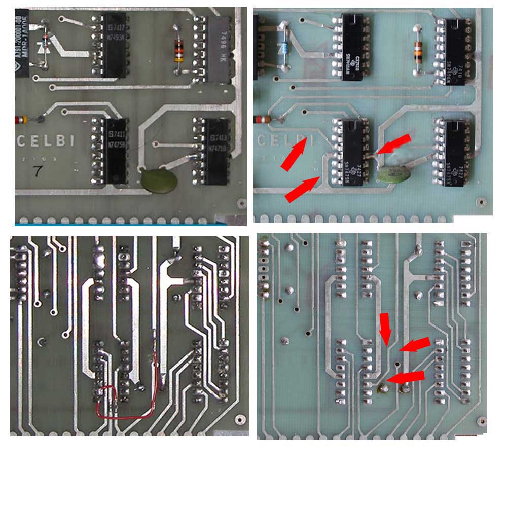
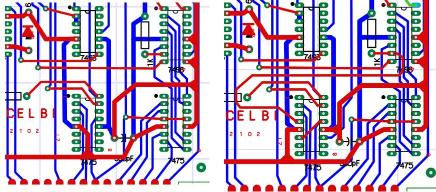
Here are partial images of the front and back of relevant sections of both boards. Red arrows on images of the Nat Wadsworth unit show where visible changes were made.

Cassette Write Board Changes

Cassette Write Board Changes

Note that the changes are somewhat different than the what was done in rework on the CHM unit. These changes don’t match the schematics, but I was able to piece together what was done and why.

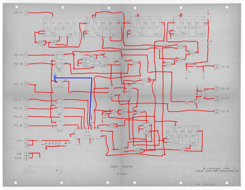
First, let’s talk a bit about what is going on, by reviewing this section of the schematics.

Cassette Schematics - Z1

Cassette Schematics – Z1

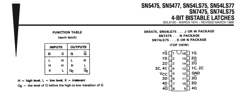
The chip associated with all these changes is a 7475, a part that has 4 bi-stable latches. Here is the key part of the data sheet – the truth table and the pinout.

7475 Data Sheet

7475 Data Sheet

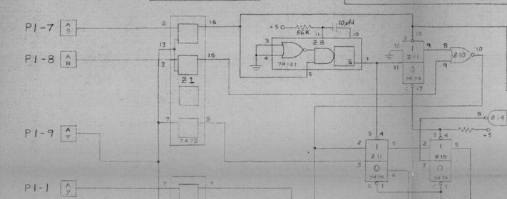
The function of this chip is pretty simple. Whenever clock input 13 is high, the chip’s output pins, 16 and 15 follow the input on pins 2 and 3, respecitively. Also, output pins 10 and 9 follow inputs 6 and 7, respectively, when clock input 4 is high. When inputs 4 or 13 go low, the associated pair of outputs, are “frozen” or are “latched” into their current state at the time the clocks inputs go low. Note that there are normal and inverted outputs for each latch.

In the schematics, three inputs are connected from a SCELBI output port to this chip. There are two data bits and the port’s output strobe. The output strobe is a high going pulse that occurs when an 8008 OUT instruction addressed to this port. The data bits are connected to the SCELBI write data bus, so will change rapidly, as the 8008 writes to memory or output ports. The strobe is connected to the clock input (pin 13) of the 7475 latches 1 and 2. This circuit allows the 7475 chip to capture 2 bits of the SCELBI output data onto latches 1 and 2 whenever an out instruction is directed to the output port connected to the cassette interface.

What about the two other latches of the 7475? In the schematics, the clock (on pin 4) for outputs 3 and 4 is not connected. What usually happens on unconnected inputs of 74XX series logic is that the input will “float” high. As mentioned before, if the clock inputs are high on the 7475, then the outputs will simply track the state of the inputs. The 3rd latch of this chip is not connected or used. However the 4th latch (pin 7) is connected to the strobe input, so the output will follow the strobe all the time. The inverted output on pin 8 is used as a clock elsewhere on the board. The function is a buffer and inverter of the strobe input to the board. Note that letting an input “float” high is not a good design practice and it’s possible that clock input on pin 4 was directly tied to +5 volts, which is connected to pin 5. It is not connected on the bottom of the board, but could be connected on the top of the board, which is obscured by the chip. The only way to know for sure, would be to use an ohm meter to determine if pin 4 is connected somewhere by a trace that is obscured by the chip. I don’t presently have access to this board, which is in storage at the CHM, so I can’t do this. My best guess, based on the extensive use of pull up’s elsewhere on the SCEBLI boards, and lack of a connection in the schematics, is that it was left to float high and was not connected.

As mentioned in the previous blog post, the first version of the layout has two significant problems.

1) The strobe output wasn’t connected to pin 7 of the 7475. This is rectified with a jumper wire.
2) The output on pin 8 (which is the inverted strobe signal), is not correctly connected to the rest of the circuit. This is rectified by a cut and jumper as can be seen in the image of the back of the board.

So what did the people at SCELBI do, to fix the problems in revised layout.

1) Power and ground connections to the chip were rerouted to make room for signal traces that needed to be added.
2) The inverted strobe output which was supposed to be on pin 8 was moved to pin 11, which is the inverted latch 3 output. This was done to make it easier to connect to the rest of the circuit. It was also disconnected from the strobe input connection.
3) The floating clock input on pin 4 was tied to an existing pull up resistor.
4) The latch 3 input was connected to strobe input by running a trace under the chip to pin 13, which was already connected to strobe. I actually can’t verify this change, but I can be fairly certain that it exists, since the circuit would not work without this trace.

Note that this change to use latch 3 instead of latch 4 for buffering and inverting the strobe is not reflected in any schematics that I have seen. The schematics actually don’t match either of the boards described in this description.

If you look at CAD images of this section of the board, you can see how the changes were made. Blue traces are on the bottom layer and red traces are on the top layer of the PCB.

Write Board Changes

Write Board Changes

I have repeated this sort of exercise numberous times over the years to solve various inconsistencies in schematics and PCB layouts in a number of vintage computers. Understanding a vintage design frequently requires detailed detective work, but with time and patience, most mysteries can be solved.

One last comment about the nature of the problems with this board. Of the thirteen SCELBI boards that I have investigated in detail, this is the first significant layout problem I have run across. There is an issue on the DBB board with a single missing trace. In this case, the connections to the 7475 were botched and had to be redone. This is a very unusual and unexpected mistake from the engineers at SCELBI.

Cassette Write Board Rework

More progress on the SCELBI cassette write board. I have figured out the reason for the rework seen on at least one board.

Cassette Write Board Rework

Cassette Write Board Rework

There are two wires and a cut on this board. In both these cases, the PCB didn’t follow the schematics. Both changes are related to chip Z1 connections.

In case 1, pin Z1-7 should have been connected to Port A, pin T. Port A, pin T is already correctly connected to Z1-13 and Z2-13 and Z2-4. I’m not sure if this omission was on purpose or not. Routing to Z1, pin 7 would require running a trace on the top of board, from Z1-13 out the top of Z1 around the outside of Z1 to Z1-7. This would also require re-routing a couple of other traces on the top side of the board to make room for this new trace. It’s very unlikely, but possible the layout person didn’t want to mess with this and decided to just require the board builder to add a wire.

In the second case, Z1-8 is not connected to Z11-3. Instead Z11-3 is connected to Port A, pin T. The fix requires cutting the trace from Port A, pin T, after it splits and runs through a via to go to Z2. Then a wire can be soldered from the cut trace to Z1-8. This is clearly a layout error.

I still have at least one more mystery to solve on the cassette write board, before I’m done with it, but the layout is shaping up real well.