Since I’m no longer making or selling Brain Boards, I’ve made the Gerber files and CAD files available for download from my website. This board has been cloned by a few different folks, but if you want to make one, it’s easier than ever.
I’m aware that Superproto WIKI is currently broken. I’ve made a couple of half hearted attempts to fix it, and will hopefully find some more time in the near future to properly repair it.
The only hard to find part, should be the MCM6571. I picked up a few, a year ago. I don’t remember off-hand where I got them, but it was probably an eBay purchase.
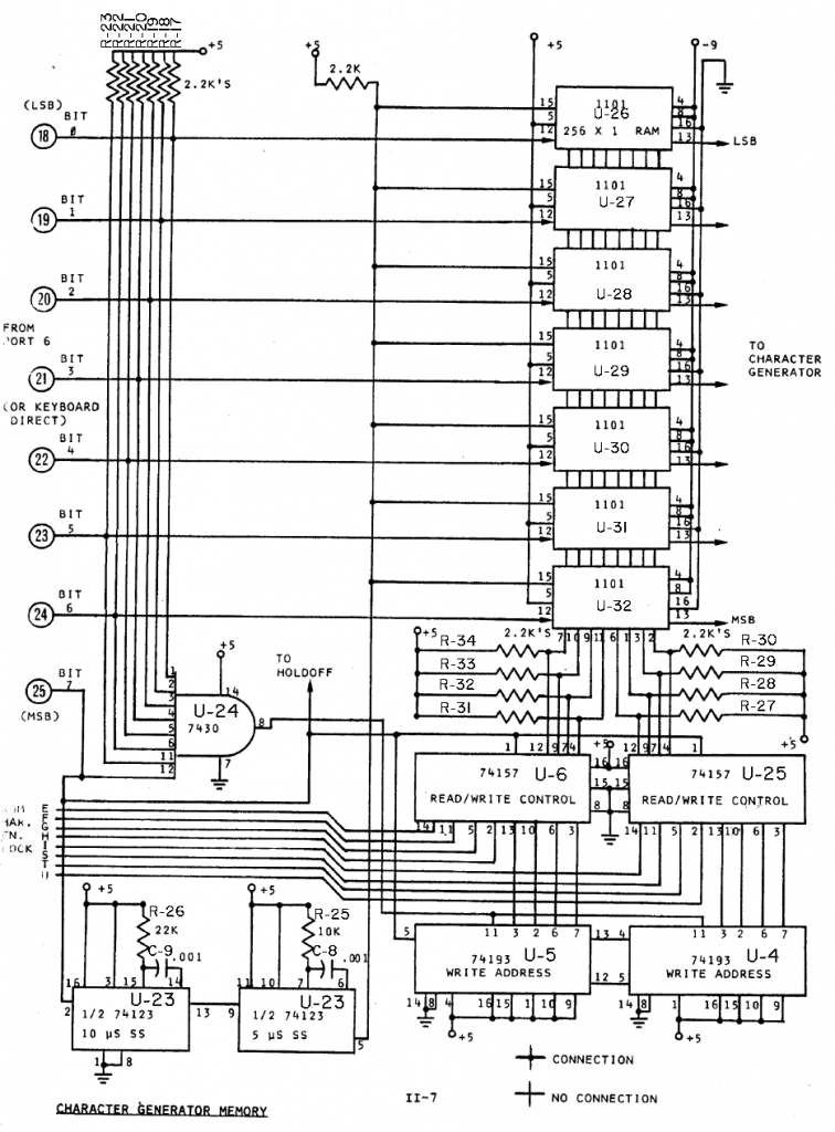
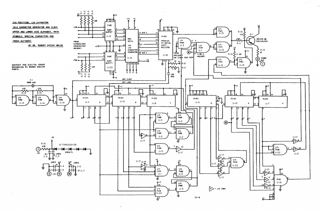
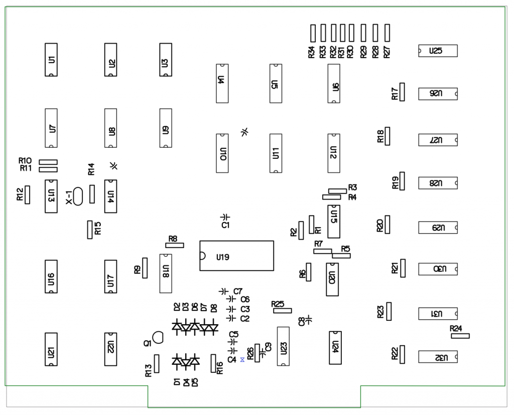
These schematics have part identifiers added to them that match the drawing that I posted yesterday. There are also a couple of corrections. A couple of the connections to the inverters at U-17 and U-21 went to different pins than what was actually connected on the PCB. No functional difference, but it could cause some confusion when debugging. One other thing, there are actually eight voltage dropping diodes, not the five shown on the schematics.
DG Video – Memory SchematicDG Video – Char Gen Schematic
Work on reproduction of this PCB card nearing the end of the CAD phase. I’ve gone through numerous design checks and think that if I had a card made with the current CAD files that I most likely will have all the connections correctly made.
I’m currently going through a final pass of making sure alignment of reproduction traces matches with the original. Though I am close to finalizing those changes, close inspection is still revealing a few adjustments that will improve fidelity to the original design.
Once I get to the point that I can’t find any more tweaks to make, I’ll pull the trigger on getting a small batch of boards made. I expect very limited demand, so this will most likely be the only batch that I make.
I’ve also created modified schematics that includes part identifiers that match what I’ve done in my CAD program. The original Digital Group schematics do not include any part identifiers. Here is what the board with identifiers currently looks like in my CAD file. Note that chip orientation is not consistent on this board, so anyone building one of these will have to work carefully to make sure chips are not inserted backwards.
Those of you who visited my SCELBI/Scopewriter exhibit at VCF east may have noticed that I was dealing with some stability problems with the Scopewriter display. I finally found some time to resolve the issue.
The Scopewriter uses a TMS3112 Static Shift Register to hold the output. The design uses a clock to circulate the text through the shift register in order to refresh the display. This is somewhat similar to the Apple 1 or TV Typewriter design. It turns out that the clock feeding from IC1, pin 10, to the TMS3112, pin 7, doesn’t meet the pulse width, clock low specification of 150ns. A quick fix that seems to work is to add a .1uF capacitor in parallel to C2, which couples these two pins.
There is another change that I made a while back in order to get the Scopewriter to work. That is adding a 470 ohm resistor in parallel to the 100K resistor, R4. I can’t remember exactly why that change was necessary, but last week, as an experiment, I removed the hacked on resistor and I couldn’t get a good display on the scope. That may be documented in one of my earlier Scopewriter posts, but I don’t have the time to figure it out. I ended up putting the resister back in place.
At this point, Scopewriter seems to be working very well with the SCELBI.
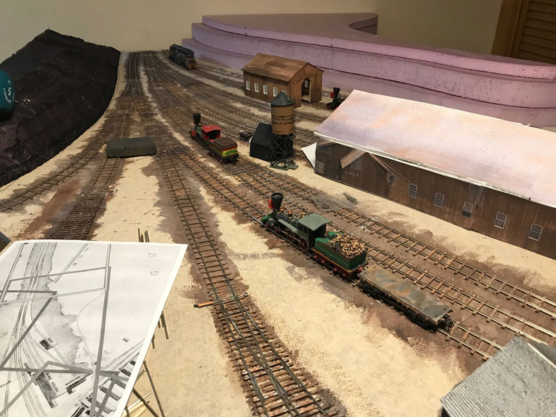
The bluffs are going up on my model railroad. You can’t really tell from this image, but it’s making a vast difference in the the appearance of this incomplete module. This really gives me motivation to move forward to see how it’s going to look with some more scenery in place.
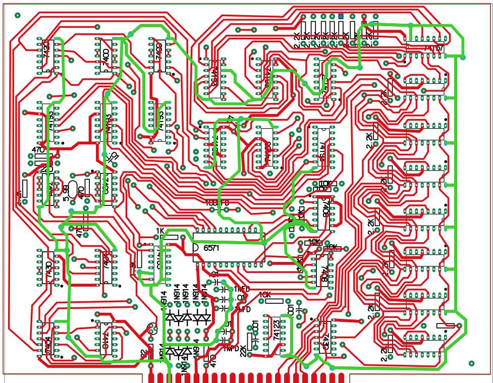
In the following image of the Digital Group Video Card, the ground traces are highlighted in green.
Digital Group Video Board (ground traces in green)
I normally I try to refrain for making severe criticisms of the boards I work to reproduce. The people who designed these products were blazing new trails, something that should be respected. However, the routing of ground traces on this board appears to be something that should avoided by people producing new designs. Note how the route to ground for the 74123 (in the bottom center) runs completely around the exterior of the board before exiting on the board edge connector, which it is almost touching. When I finally build one up, I wouldn’t be surprised if I have ground issues with this design. The good news is that it should be pretty easy to resolve any issues that do crop up.
I have quite a bit of fine tuning and clean up to do before ordering a PCB, but as you can see by viewing the layout image in this post, the hardest part of the work is done. The existing schematics don’t have any kind of chip ID or location, other than part type. I’ll be rectifying this and be publishing a parts list, chip placement diagram and updated schematics, by the time I’m done with this project.
I discovered one other issue that I’ll have to deal with. The 6571 character generator needs a +12 volt supply. For now, I can use a separate 12 volt lab supply. I think I’ll have to create some kind boost converter to generate +12 from the +5 volt supply by the time I’m done with this project.
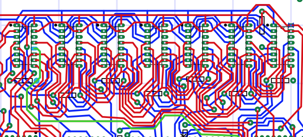
I’ve been working on reproducing the a copy of the Digital Group video card. In the process, I have found that the layout of the board is pretty convoluted in some places. In particular, the layout for the seven 1101 memory chips is pretty messy. Though, it is far from complete, the traces are all in place and you can see approximately what this part of the completed design will look like by viewing the following image.
Digital Group Video Card 1100 SRAM Layout
Take a look at how the traces wind around the outside of the chips. Circuit board design was done by hand back in those days. The layout is made by making an image of the PCB on a piece of film that will be reproduced by photographic imaging. Each small section of straight trace is laid onto a piece of film by cutting an appropriate length of tape and laying it down on the film. Though the size is typically 2X the final size of the PCB, which makes things a little easier, it is still a time consuming process. With this many changes in direction for each trace, I can’t imagine how long it took the layout artist to produce the original artwork. Even digitally, it is taking quite a while for me to reproduce.
For quite a different approach to the same problem, take a look at the layout of 1 bank of the SCELBI 1K SRAM card, which uses the same 1101 memory chips. In this case almost all traces run in straight lines, making for a much easier layout process.
SCELBI 1101 SRAM Bank Layout
So why is there so much a difference? The Digital Group card has absolutely no traces running between the pads of a chip. I presume they did this in order to make the design a little more robust as tolerances can be a bit tight when you run traces between the small gaps between the legs of a chip. Tight tolerances can result in higher likelihood of PCB manufacturing defects or solder shorts during the assembly process. However, by making the small sacrifice of tighter tolerances, you can see that there is great improvement in the resulting design.
I’ve released a new version of my OS/X SCELBI app.
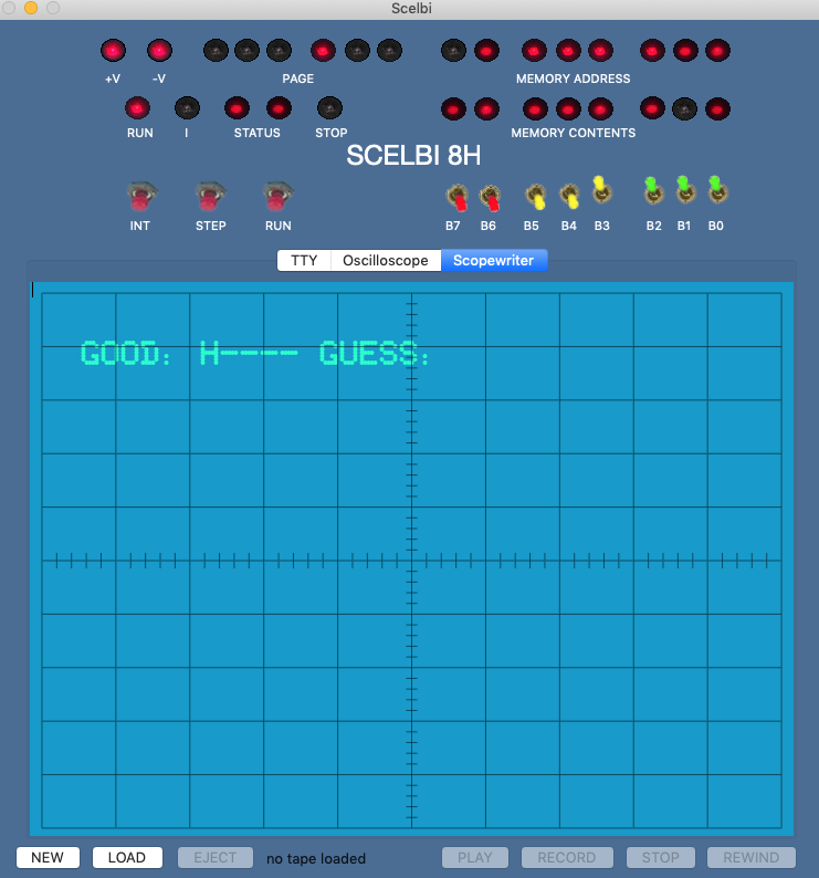
Scelbi App with Scopewriter Interface
This version incorporates support for the SCELBI Scopewriter interface. This support is pretty barebones, and doesn’t include emulated hardware timing. While any real SCELBI Scopewriter application will work in this emulator, because timing is not emulated, applications developed in the emulator may not work on the real thing.
The second feature added, is integrated support for a 256 byte EPROM in the 4K/8H mode. There are two versions of the EPROM included. First EPROM image is a MCMON monitor with a 2400 baud bit banged serial driver. The second EPROM image is different version of the MCMON monitor that includes support for keyboard and the Scopewriter.
But that’s not all, in order to demo the Scopewriter with the SCELBI, I have SCELBI’s hangman game going on both versions of MCMON. It is also downloadable from my 8008 applications page.
Progress on the City Point Model Railroad layout has been stalled for quite some time while I figured out the best way to etch a PCB that I want to use for the switch control panel. I have etched many PCBs in the past, but this one is much larger than the small boards that I have etched in the past and didn’t have a large enough tank or enough etchant solution. Sure, I could have just purchased a suitable tank, but I really didn’t want to add to much to the clutter that seems to add up around here.
Finally I gave in and went to Walmart and purchased a large flat bottomed storage tub. This new tub would be large enough to hold the etchant and PCB while etching. However, I still didn’t have enough etchant to fill the tub high enough to cover the PCB. Yesterday, I figured out that if I cut the edges off of the cover, which had a large flat bottomed depression in the middle, that the cover of the tub might work better and require less etchant. As it turns out, all I had to do, was to pour warm ferric chloride etchant onto the PCB and roll it around a bit, catching any run off in the tub. After about a half dozen passes, the PCB was etched. This was much easier to accomplish than I had expected.
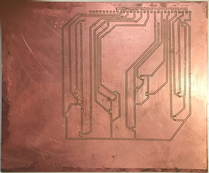
Switch Control Panel Back
The result is far from my best work, but it will have to do.
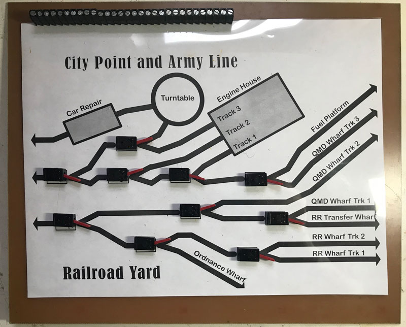
The switches and connectors will be mounted on the reverse side of the PCB along with the graphics, which will be covered by a transparency that should help prevent wear and improve the look. I think these toggle switches will make selecting a route very intuitive. It also removes the need to add LEDs to indicate the selected route.
Switch Control Panel
I need to print off a colored copy of the artwork before I frame it. Once framed, I’ll mount it on the fascia of the layout. After it’s mounted, wiring to the switch machines should be very straight forward.