
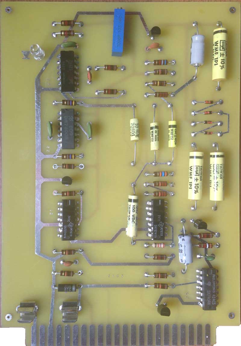
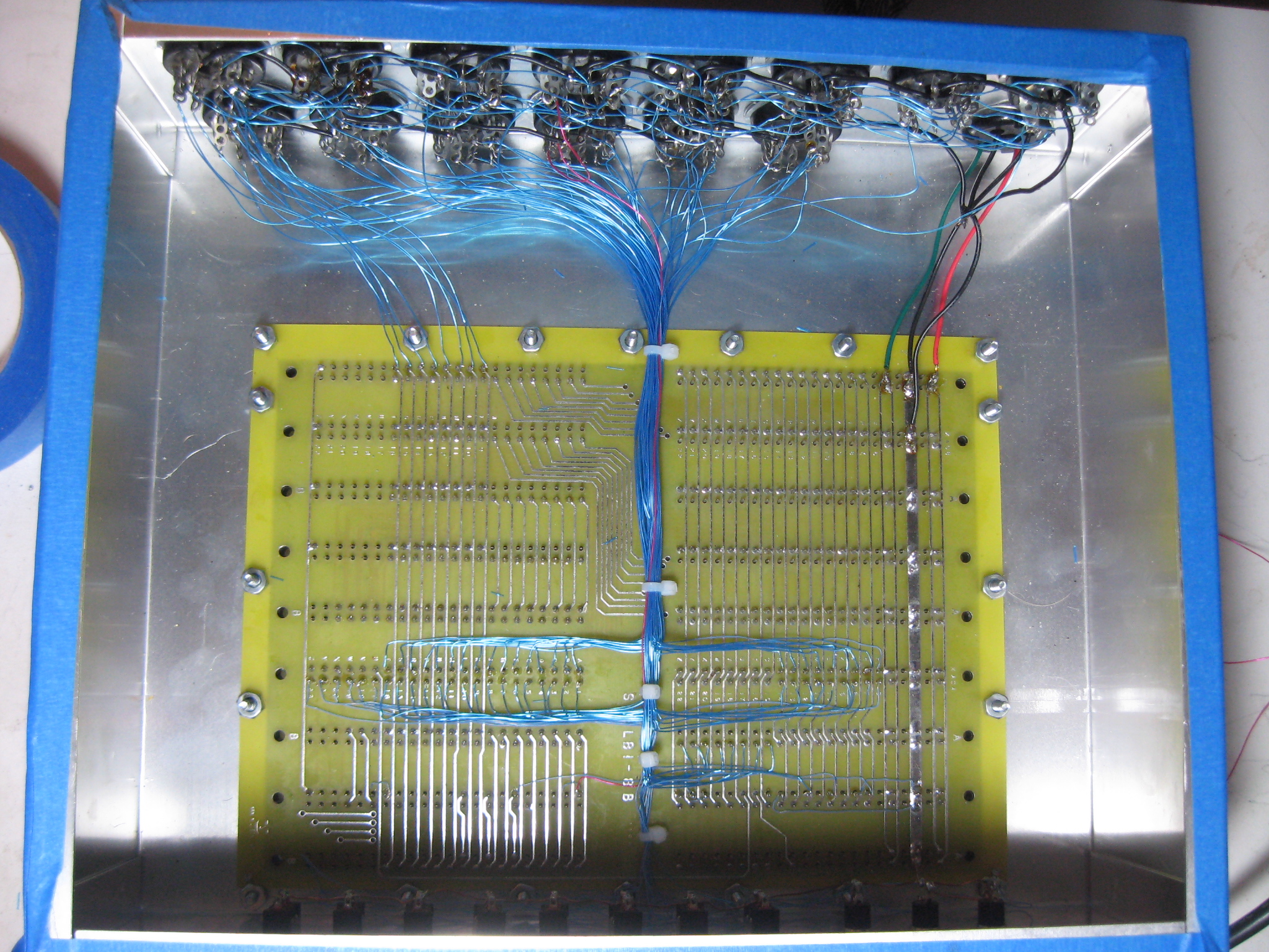
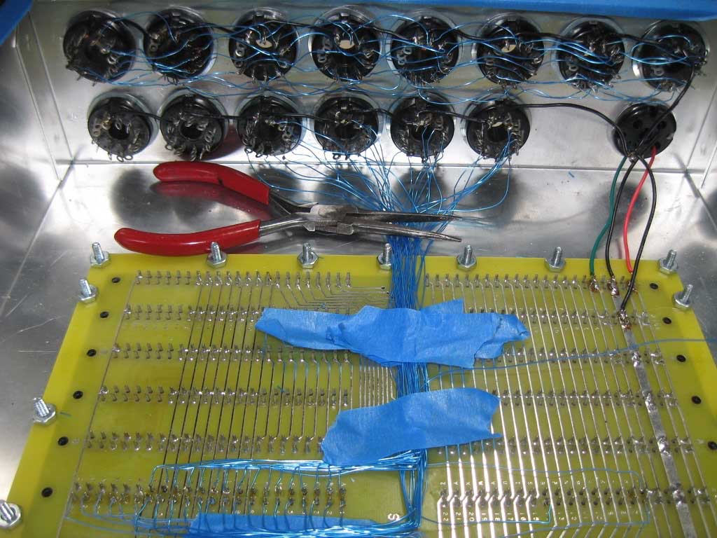
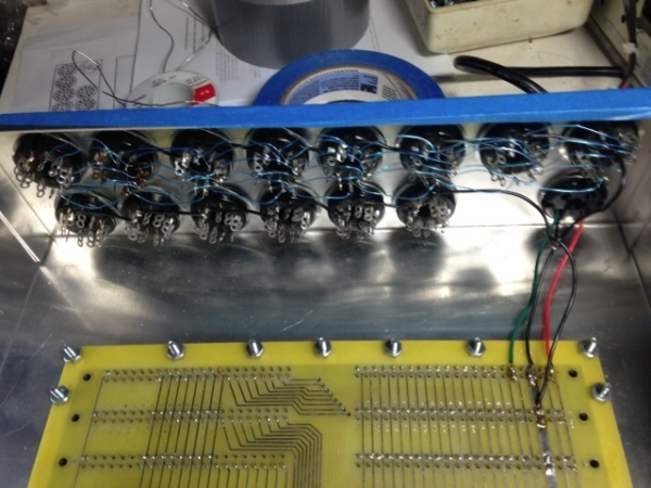
SCELBI Cassette Read Card
Since I didn’t have information on the transistors used, I choose vanilla 2N3904 (NPN) and 2N3906 (PNP) transistors for this build. The 72741 OP-AMPs are vanilla 741 OP-AMPs in a 14 pin package. They are pretty hard to find in that package, but I did manage to snag a few off of eBay. I described where I found the yellow capacitors in a previous post. You will notice one carbon film resistor in the mix. That is because I forgot to order a 2700 ohm composition resistor, and I happened to have the right value carbon film resistor in my stash.
This card is essentially just a tone detector. I should be able to test functionality and performance and adjust it without hooking it up to my SCELBI by using a computer based tone generator application that I bought a while back. This is what I did when resurrecting the HAL ST-6 TTY terminal unit. Except for frequencies used, it basically does the same thing, though at a much less sophisticated level.
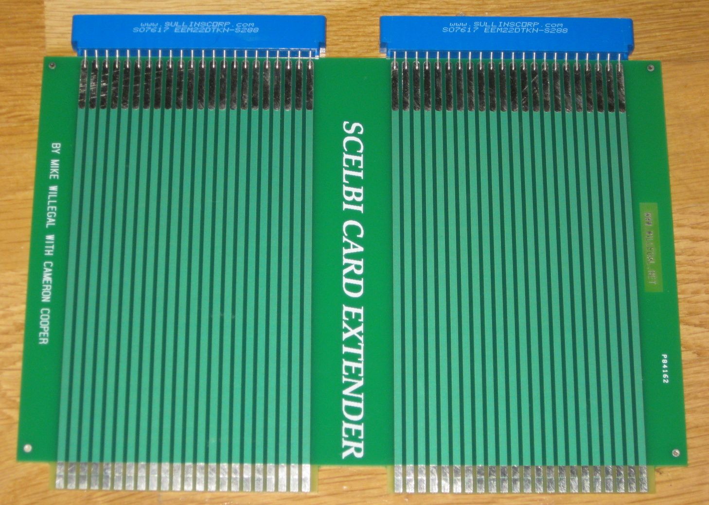
One unique thing about this board is that there isn’t a single VIA present.